ZHCSI30G March 2002 – April 2018 OPA2354 , OPA354 , OPA4354
PRODUCTION DATA.
- 1 特性
- 2 应用
- 3 说明
- 4 修订历史记录
- 5 Device Comparison Table
- 6 Pin Configuration and Functions
- 7 Specifications
- 8 Detailed Description
- 9 Application and Implementation
- 10Power Supply Recommendations
- 11Layout
- 12器件和文档支持
- 13机械、封装和可订购信息
11.5 PowerPAD Assembly Process
The PowerPAD must be connected to the most negative supply voltage for the device, which is ground in single-supply applications and V− in split-supply applications.
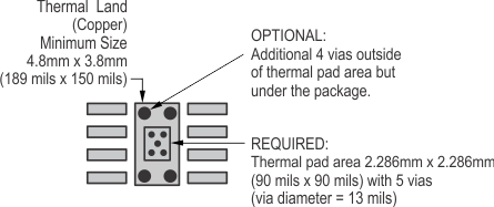
Prepare the PCB with a top-side etch pattern, as shown in Figure 41. The exact land design may vary based on the specific assembly process requirements. There must be etch for the leads and etch for the thermal land.
Place the recommended number of plated-through holes (or thermal vias) in the area of the thermal pad. These holes must be 13 mils (.013 in) in diameter. The holes are small so that solder wicking through the holes is not a problem during reflow. TI recommends a minimum of five holes for the 8-pin HSOP PowerPAD package, as shown in Figure 41.
 Figure 41. 8-Pin PowerPAD PCB Etch and Via Pattern
TI recommends, but does not require, placing a small number of additional holes under the package and outside the thermal pad area. These holes provide additional heat paths between the copper thermal land and the ground plane. The holes may be larger because the holes are not in the area to be soldered, so wicking is not a problem. This technique is shown in Figure 41.
Connect all holes, including those within the thermal pad area and outside the pad area, to the internal ground plane or other internal copper plane for single-supply applications, and to V− for split-supply applications.
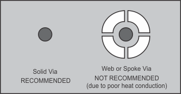
When laying out these holes, do not use the typical web or spoke via connection methodology, as shown in Figure 42. Web connections have a high thermal resistance connection that is useful for slowing the heat transfer during soldering operations. This feature makes soldering the vias that have ground plane connections easier. However, in this application, low thermal resistance is desired for the most efficient heat transfer. Therefore, the holes under the PowerPAD package must make connection to the internal ground plane with a complete connection around the entire circumference of the plated-through hole.
 Figure 42. Via Connection
The top-side solder mask must leave the pad connections and the thermal pad area exposed. The thermal pad area must leave the 13-mil holes exposed. The larger holes outside the thermal pad area may be covered with a solder mask.
Apply solder paste to the exposed thermal pad area and all of the package pins.
With these preparatory steps in place, the PowerPAD device is placed in position and run through the solder reflow operation as any standard surface-mount component. This preparation and processing results in a part that is properly installed.
For detailed information on the PowerPAD package, including thermal modeling considerations and repair procedures, see PowerPAD Thermally Enhanced Package on www.ti.com.