ZHCS042C April 2011 – March 2021 OPA2376-Q1 , OPA376-Q1 , OPA4376-Q1
PRODUCTION DATA
- 1 特性
- 2 应用
- 3 说明
- 4 Revision History
- 5 Pin Configuration and Functions
- 6 Specifications
- 7 Detailed Description
- 8 Application and Implementation
- 9 Power Supply Recommendations
- 10Layout
- 11Device and Documentation Support
- 12Mechanical, Packaging, and Orderable Information
5 Pin Configuration and Functions
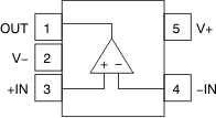 Figure 5-1 OPA376-Q1: DBV (5-Pin SOT-23) Package, Top View
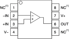
(1) NC denotes no internal connection.
Figure 5-3 OPA376-Q1: D (8-Pin SOIC) Package, Top View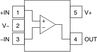 Figure 5-2 OPA376-Q1: DCK (5-Pin SC70) Package, Top View
Table 5-1 Pin Functions: OPA376-Q1
| PIN | I/O | DESCRIPTION | |||
|---|---|---|---|---|---|
| NAME | NO. | ||||
| SOT-23 | SC70 | SOIC | |||
| +IN | 3 | 1 | 3 | I | Noninverting input+ |
| –IN | 4 | 3 | 2 | I | Inverting input– |
| NC | — | — | 1, 5, 8 | — | No internal connection |
| OUT | 1 | 4 | 6 | O | Output |
| V+ | 5 | 5 | 7 | — | Positive (highest) power supply+ |
| V– | 2 | 2 | 4 | — | Negative (lowest) power supply– |
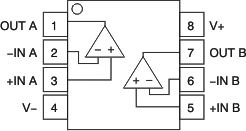 Figure 5-4 OPA2376-Q1: D (8-Pin SOIC) and DGK (8-Pin VSSOP) Packages, Top View
Table 5-2 Pin Functions: OPA2376-Q1
| PIN | I/O | DESCRIPTION | |
|---|---|---|---|
| NAME | NO. | ||
| +IN A | 3 | I | Noninverting input, channel A+ |
| –IN A | 2 | I | Inverting input, channel A– |
| +IN B | 5 | I | Noninverting input, channel B+ |
| –IN B | 6 | I | Inverting input, channel B– |
| OUT A | 1 | O | Output, channel A |
| OUT B | 7 | O | Output, channel B |
| V– | 4 | — | Negative (lowest) power supply |
| V+ | 8 | — | Positive (highest) power supply |
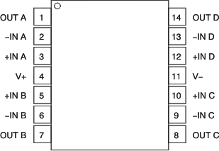 Figure 5-5 OPA4376-Q1: PW (14-Pin TSSOP) Package, Top View
Table 5-3 Pin Functions: OPA4376-Q1
| PIN | I/O | DESCRIPTION | |
|---|---|---|---|
| NAME | NO. | ||
| +IN A | 3 | I | Noninverting input, channel A+ |
| –IN A | 2 | I | Inverting input, channel A– |
| +IN B | 5 | I | Noninverting input, channel B+ |
| –IN B | 6 | I | Inverting input, channel B– |
| +IN C | 10 | I | Noninverting input, channel C+ |
| –IN C | 9 | I | Inverting input, channel C– |
| +IN D | 12 | I | Noninverting input, channel D+ |
| –IN D | 13 | I | Inverting input, channel D– |
| OUT A | 1 | O | Output, channel A |
| OUT B | 7 | O | Output, channel B |
| OUT C | 8 | O | Output, channel C |
| OUT D | 14 | O | Output, channel D |
| V+ | 4 | — | Positive (highest) power supply |
| V– | 11 | — | Negative (lowest) power supply |