SBOS406G June 2007 – December 2015 OPA2376 , OPA376 , OPA4376
PRODUCTION DATA.
8 Application and Implementation
NOTE
Information in the following applications sections is not part of the TI component specification, and TI does not warrant its accuracy or completeness. TI’s customers are responsible for determining suitability of components for their purposes. Customers should validate and test their design implementation to confirm system functionality.
8.1 Application Information
The OPA376 family of operational amplifiers is built using e-trim, a proprietary technique in which offset voltage is adjusted during the final steps of manufacturing. This technique compensates for performance shifts that can occur during the molding process. Through e-trim, the OPA376 family delivers excellent offset voltage (5 μV, typical). Additionally, the amplifier boasts a fast slew rate, low drift, low noise, and excellent PSRR and AOL. These 5.5-MHz CMOS op amps operate on 760-μA (typical) quiescent current.
8.1.1 Basic Amplifier Configurations
The OPA376 family is unity-gain stable. It does not exhibit output phase inversion when the input is overdriven. A typical single-supply connection is shown in Figure 25. The OPA376 is configured as a basic inverting amplifier with a gain of –10 V/V. This single-supply connection has an output centered on the common-mode voltage, VCM. For the circuit shown, this voltage is 2.5 V, but may be any value within the common-mode input voltage range.
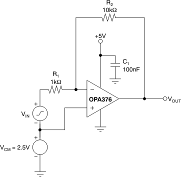 Figure 25. Basic Single-Supply Connection
8.1.2 Active Filtering
The OPA376 series is well-suited for filter applications requiring a wide bandwidth, fast slew rate, low-noise, single-supply operational amplifier. Figure 26 shows a 50-kHz, 2nd-order, low-pass filter. The components have been selected to provide a maximally-flat Butterworth response. Beyond the cutoff frequency, roll-off is –40 dB/decade. The Butterworth response is ideal for applications requiring predictable gain characteristics such as the anti-aliasing filter used ahead of an analog-to-digital converter (ADC).
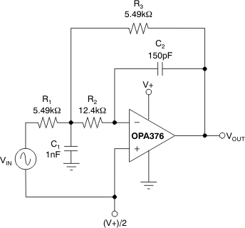 Figure 26. Second-Order, Butterworth, 50-kHz, Low-Pass Filter
8.1.3 Driving an Analog-to-Digital Converter
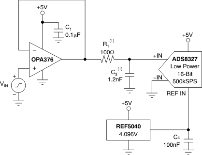
The low noise and wide gain bandwidth of the OPA376 family make it an ideal driver for ADCs. Figure 27 illustrates the OPA376 driving an ADS8327, a 16-bit, 250-kSPS converter. The amplifier is connected as a unity-gain, non-inverting buffer.
8.1.4 Phantom-Powered Microphone
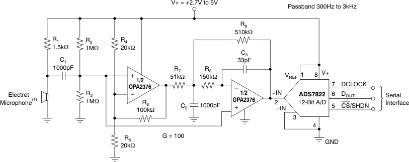
The circuit shown in Figure 28 depicts how a remote microphone amplifier can be powered by a phantom source on the output side of the signal cable. The cable serves double duty, carrying both the differential output signal from and dc power to the microphone amplifier stage.
An OPA2376 serves as a single-ended input to a differential output amplifier with a 6-dB gain. Common-mode bias for the two op amps is provided by the dc voltage developed across the electret microphone element. A
48-V phantom supply is reduced to 5.1 V by the series 6.8-kΩ resistors on the output side of the cable, and the 4.7-kΩ resistor and zener diode on the input side of the cable. AC coupling blocks the different dc voltage levels from each other on each end of the cable.
An INA163 instrumentation amplifier provides differential inputs and receives the balanced audio signals from the cable. The INA163 gain may be set from 0 dB to 80 dB by selecting the RG value. The INA163 circuit is typical of the input circuitry used in mixing consoles.
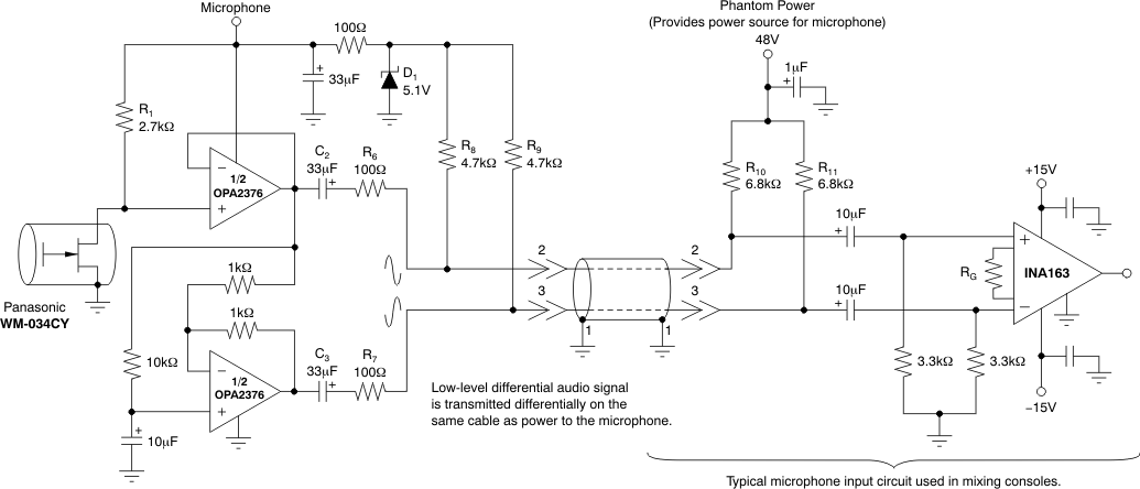 Figure 28. Phantom-Powered Electret Microphone
NOINDENT:
Electret microphone powered by R1.8.2 Typical Application
Low-pass filters are commonly employed in signal processing applications to reduce noise and prevent aliasing. The OPA376 is ideally suited to construct high-speed, high-precision active filters. Figure 30 shows a second-order, low-pass filter commonly encountered in signal processing applications.
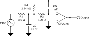 Figure 30. Typical Application Schematic
8.2.1 Design Requirements
Use the following parameters for this design example:
- Gain = 5 V/V (inverting gain)
- Low-pass cutoff frequency = 25 kHz
- Second-order Chebyshev filter response with 3-dB gain peaking in the passband
8.2.1.1 Detailed Design Procedure
The infinite-gain multiple-feedback circuit for a low-pass network function is shown in Figure 30. Use Equation 1 to calculate the voltage transfer function.

This circuit produces a signal inversion. For this circuit, the gain at dc and the low-pass cutoff frequency are calculated by Equation 2:

Software tools are readily available to simplify filter design. WEBENCH® Filter Designer is a simple, powerful, and easy-to-use active filter design program. The WEBENCH Filter Designer lets you create optimized filter designs using a selection of TI operational amplifiers and passive components from TI's vendor partners.
Available as a web based tool from the WEBENCH® Design Center, WEBENCH® Filter Designer allows you to design, optimize, and simulate complete multistage active filter solutions within minutes.
8.2.2 Application Curve
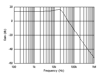 Figure 31. Low-Pass Filter Transfer Function