SBOS391B December 2007 – March 2016 OPA454
PRODUCTION DATA.
- 1 Features
- 2 Applications
- 3 Description
- 4 Revision History
- 5 Device Comparison Table
- 6 Pin Configuration and Functions
- 7 Specifications
- 8 Parameter Measurement Information
- 9 Detailed Description
- 10Application and Implementation
- 11Power Supply Recommendations
- 12Layout
- 13Device and Documentation Support
- 14Mechanical, Packaging, and Orderable Information
10 Application and Implementation
NOTE
Information in the following applications sections is not part of the TI component specification, and TI does not warrant its accuracy or completeness. TI’s customers are responsible for determining suitability of components for their purposes. Customers should validate and test their design implementation to confirm system functionality.
10.1 Applications Information
The OPA454 is a high-voltage, high-current operational amplifier capable of operating with supply voltages as high as ±50 V, or as low as ±10 V. Its design and processing allows it to be used in applications where most operational amplifiers cannot be used because of high-voltage power supply conditions, or as a result of the need for very high-output voltage swing. The output is capable of swinging within a volt, to a few volts, of the supply rails depending on the output current, which can be as much as ±50 mA. In addition, the OPA454 features input overvoltage protection, built-in output current limiting, thermal protection, and an output enable/disable function.
10.1.1 Lowering Offset Voltage and Drift
The OPA454 can be used with an OPA735 zero-drift series op amp to create a high-voltage op amp circuit that has very low input offset temperature drift. This circuit is shown in Figure 64.
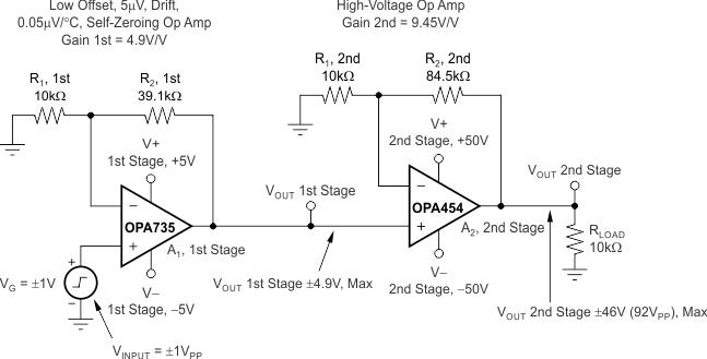 Figure 64. Two-Stage, High-Voltage Op Amp Circuit with Very Low Input Offset Temperature Drift
10.1.2 Increasing Output Current
The OPA454 drives an output current of a few milliamps to greater than 50 mA while maintaining good op amp performance. See Figure 6 for open-loop gain versus temperature at various output current levels.
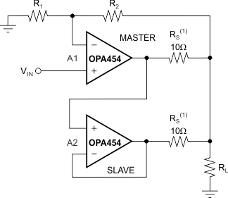
In applications where the 25-mA output current is not sufficient to drive the required load, the output current can be increased by connecting two or more OPA454s in parallel, as Figure 65 shows. Amplifier A1 is the master amplifier and may be configured in virtually any op amp circuit. Amplifier A2, the slave, is configured as a unity-gain buffer. Alternatively, external output transistors can be used to boost output current. The circuit in Figure 66 is capable of supplying output currents up to 1 A, with the transistors shown.
NOINDENT:
RS resistors minimize the circulating current that always flows between the two devices because of VOS errors.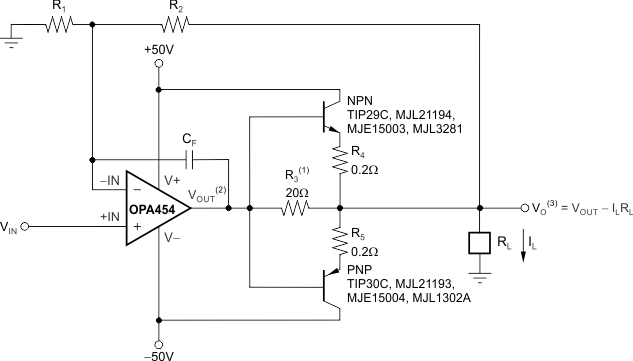
NOINDENT:
Provides current limit for OPA454 and allows the amplifier to drive the load when the output is between +0.7 V and –0.7 V.NOINDENT:
Op amp VOUT swings from +47 V to –48 V.NOINDENT:
VO swings from +44.1 V to –45.1 V at IL = 1 A.10.1.3 Unity-Gain Noninverting Configuration
When in the noninverting unity-gain configuration, the OPA454 has more gain peaking with increasing positive common-mode voltage and increasing temperature. It has less gain peaking with more negative common-mode voltage. As with all op amps, gain peaking increases with increasing capacitive load. A resistor and small capacitor placed in the feedback path can reduce gain peaking and increase stability.
10.2 Typical Application
Figure 67 shows the OPA454 in a typical noninverting application with output voltage boost.
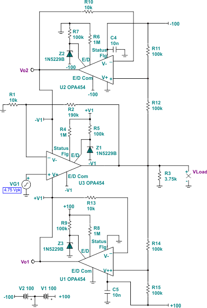 Figure 67. OPA454 Noninverting, AV = 20 V/V, Output Voltage Boost
10.2.1 Design Requirements
Figure 67 shows an output voltage boost circuit where three OPA454 op amps connected as shown can produce an output voltage swing as high as 195 VPP. The resulting output swing range is twice that attainable with a single OPA454 device operating from ±50-V supplies, and is useful in applications where an even higher output swing is required. A ±100-VDC power supply is required for this configuration.
Three of the design goals for this circuit are:
- A noninverting gain of 20 V/V (26 dB)
- A peak output voltage approaching 97.5 V, while delivering a peak output current of approximately 24 mA
- Correct biasing of the Enable/Disable (E/D), E/D Com, and Status flag pins
10.2.2 Detailed Design Procedure
U3 (an OPA454) is the only amplifier of the three devices in the application that is responsible for signal amplification. The other two op amps, U1 and U2, provide the positive and negative supply sources (respectively) for U3. The voltage gain of U3 is that of a traditional noninverting op amp amplifier. A simple relation involving U3 feedback (R2) and input (R1) resistors sets the closed-loop gain, AV. Equation 1 shows this calculation.

where
- R1 = 10 kΩ
- R2 = 190 kΩ
- AV = 20 V/V
Applying this gain and a VPK of ±97.5 V, the maximum input voltage that may be applied without causing the output to clip is ±4.75 V.
U1 and U2 are connected as unity-gain buffers. The purpose of this configuration is to track the U3 output voltage, and then adjust the voltage levels at the U3 V+ and V– pins so that 100 V is maintained across them. This input is accomplished by the U1 and U2 input connection to the U3 output voltage through the 100-kΩ voltage dividers formed by R11, R12, and R14, R15. For example, as the output of U3 moves more positive, the voltage on the U1 noninverting input moves up more closely to the +100-V supply level. Even though U2 provides the U1 V– supply, its output moves more positive as well. The result is that all the devices move together in unison up and down, while maintaining the 100-V difference between the V+ and V– pins for U3.
Figure 68 shows how the U3 op amp output voltage VLOAD moves upward, becoming more positive, as the input voltage VG1 increases from –4.75 V to 4.75 V. Figure 68 also shows VO1 and VO2, the U1 and U2 (respectively) output voltages. The 100-V difference between the supply pins is evident in the graph. Notice how the U3 V+ pin (VO1) allows 100 V greater than its V– pin (VO2).
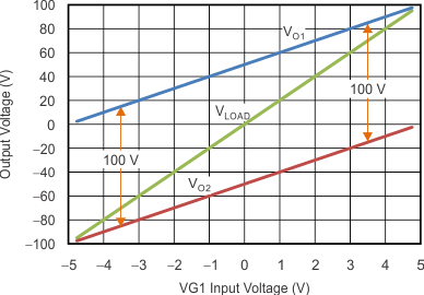 Figure 68. OPA454 Output Voltage Levels vs VS1 Input Voltage
Figure 69 shows the VLOAD output, a 195-VPP, 20-kHz sine wave, as developed across the 3.75-kΩ load resistor. The peak current provided by the OPA454 U3 output is 26 mA. U1 and U2 alternately source and sink the output current, in addition to the operating current required by U3.
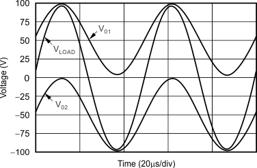 Figure 69. Output Voltage Boost Develops 195-VPP VLOAD Across 3.75-kΩ Load Resistance
The output voltage booster may be used in an inverting configuration also. This use is easily accomplished by applying the input signal to the input resistor R1 as seen in Figure 70. The noninverting input is grounded and the ratio of feedback resistor R2 to R1 is set to 20:1 to satisfy the inverting gain equation given in Equation 2.

where
- R1 = 10 kΩ
- R2 = 200 kΩ
- AV = –20 V/V
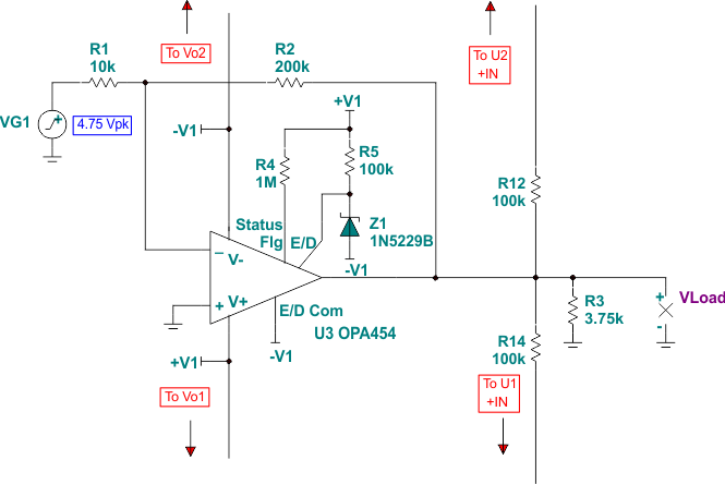 Figure 70. OPA454 Output Boost Circuit Applied as an Inverting Amplifier
10.2.3 Application Curve
Figure 71 shows an example of the inverting output boost amplifier output waveforms obtained from a TINA-TI simulation.

10.3 System Examples
10.3.1 Basic Noninverting Amplifier
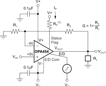
Figure 72 shows the OPA454 connected as a basic noninverting amplifier. The OPA454 can be used in virtually any ±5-V to ±50-V op amp configuration. It is especially useful for supply voltages greater than 36 V.
Power-supply terminals must be bypassed with 0.1-μF (or greater) capacitors, located near the power-supply pins. Be sure that the capacitors are appropriately rated for the power-supply voltage used.
10.3.2 Programmable Voltage Source
Figure 73 illustrates the OPA454 in a programmable voltage source.
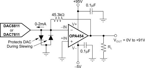 Figure 73. Programmable Voltage Source
10.3.3 Bridge Circuit
Figure 74 shows the OPA454 in a bridge circuit.
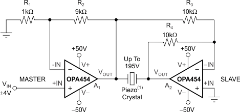
NOINDENT:
For transducers with large capacitance, stabilization may become an issue. Be certain that the Master amplifier is stable before stabilizing the Slave amplifier.10.3.4 High-Compliance Voltage Current Sources
This section describes four different applications using high-compliance voltage current sources with differential inputs. Figure 75 shows a high-voltage difference amplifier circuit. Figure 76 and Figure 78 illustrate the different applications.
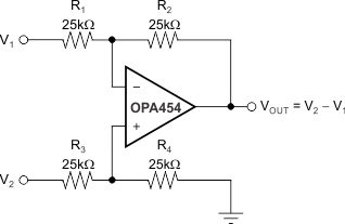 Figure 75. High-Voltage Difference Amplifier
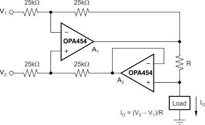 Figure 76. Differential Input Voltage-to-Current Converter for Low IOUT
A red light emitting diode (LED) was used to generate Figure 77.
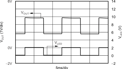 Figure 77. Avalanche Photodiode Circuit
Gain of the avalanche photodiode (APD) is adjusted by changing the voltage across the APD. Gain starts to increase when reverse voltage is increased beyond 130 V for this APD diode. See Figure 78.
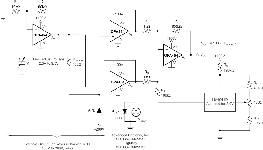 Figure 78. APD Gain Adjustment Using the OPA454, High-Voltage Op Amp
10.3.5 High-Voltage Instrumentation Amplifier
Figure 79 uses three OPA454s to create a high-voltage instrumentation amplifier. VCM ± VSIG must be between (V–) + 2.5 V and (V+) – 2.5 V. The maximum supply voltage equals ±50 V or 100 V total.
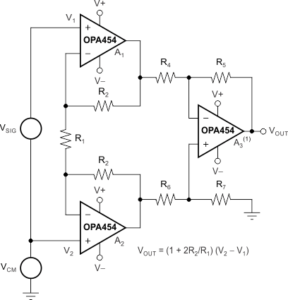
NOINDENT:
The linear input range is limited by the output swing on the input amplifiers, A1 and A2.
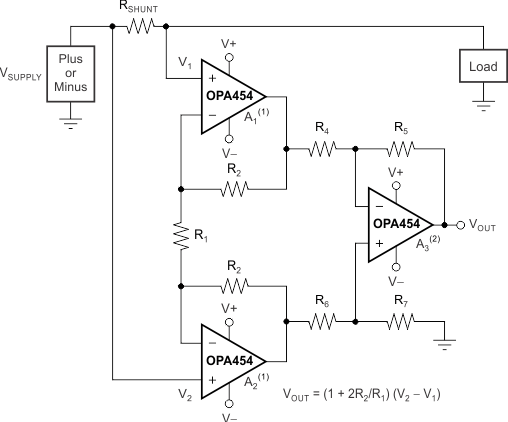
Figure 80 uses three OPA454s to measure current in a high-side shunt application. VSUPPLY must be greater than VCM. VCM must be between (V–) + 2.5 V and (V+) – 2.5 V. Adhering to these restrictions keeps V1 and V2 within the voltage range required for linear operation of the OPA454. For example, if V+ = 50 V and V– = 50 V, then
V1 = +47.5 V (maximum) and V2 = –47.5 V (minimum). The maximum supply voltage equals ±50 V, or 100 V total.
NOINDENT:
To increase the linear input voltage range, configure A1 and A2 as unity-gain followers.NOINDENT:
The linear input range is limited by the output swing on the input amplifiers, A1 and A2.Figure 81 shows an example circuit that uses the OPA454 in an output voltage boost configuration with six op amp output stages.
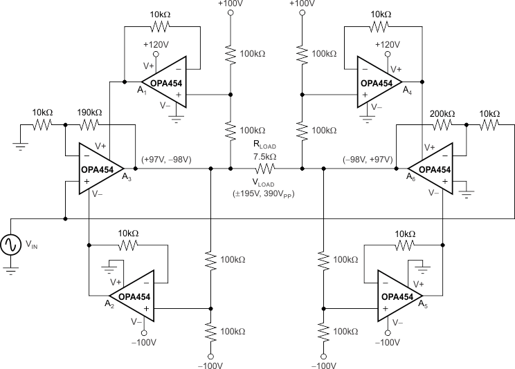 Figure 81. Output Voltage Boost with ±195 V (390 VPP) Across Bridge-Tied Load
 (Six Op Amps, see Figure 82 and Figure 83)
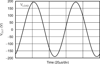 Figure 82. 390 VPP Across 7.5-kΩ Load
20 kHz, Uses Six OPA454s, 100-V Supplies
