ZHCSOX1 October 2020 OPA455
PRODUCTION DATA
- 1 特性
- 2 应用
- 3 说明
- 4 Revision History
- 5 Pin Configuration and Functions
- 6 Specifications
- 7 Detailed Description
- 8 Application and Implementation
- 9 Power Supply Recommendations
- 10Layout
- 11Device and Documentation Support
- 12Mechanical, Packaging, and Orderable Information
8.2.2.2 Detailed Design Procedure
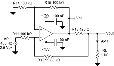
The improved Howland current pump circuit is illustrated in Figure 8-3. The OPA455 sources an output current of 20 mA when a low-voltage single-ended, 2.5-V reference voltage is applied to the circuit input. The source could be an actual 2.5-V precision reference. If the current-pump output current requires being set to different levels, a voltage output DAC can be used. If the input voltage polarity is reversed, the output current reverses direction, and 20 mA is sunk from the load through the OPA455 output.
The circuit provides the resistance values required to obtain a ±20-mA output current with the 2.5-V input voltage applied. The following can be used to select the resistors, thus setting the voltage gain and output current.
- R13 sets the gain, and is adjusted by the ratio of R14 / R15
- Selecting a low value for R13 enables all other resistors to be high, limiting current through the feedback network
- The ratio of R11 / (R12 + R13) must equal R14 / R15
- If R14 = R15, then R12 = R11 – R13
Applying these relationships the resistors are selected or derived as follows:
- Let R14 = R15 = 100 kΩ
- R13 = [(VP – VN) (R15 / R14)] / IL = [(2.5 V – 0 V) (100 kΩ / 100 kΩ)] / 0.02 A = 125 Ω
- R12 = (R11 – R13) = (100 kΩ – 125 Ω) = 99.875 kΩ
Verifying R11 / (R12 + R13) must equal R14 / R15 requirement:
- R12 = [R11(R15 / R14)] – R13 = [100 kΩ (100 kΩ / 100 kΩ)] – 125 Ω = 99.875 kΩ
The resistor values for R11 through R15 are seen in the circuit drawing.
The load is set to be 500 Ω, the sourced output current through the load is 20 mA, and the output voltage is 10 V. The voltage directly at the OPA455 output 2.5 V higher, or 12.5 V, which compensates for the voltage drop across the 125-Ω R13 resistor. If needed., a feedback capacitor can be added to reduce the ac bandwidth of the improved Howland current pump circuit. In this example, no capacitor is used.
The improved Howland current pump output is limited to the combined effects of the OPA455 linear output voltage swing range, the voltage drop developed across R13, and the voltage drop developed across load. For a particular output current, a maximum output voltage span can be achieved. This span is referred to as the output voltage compliance range.
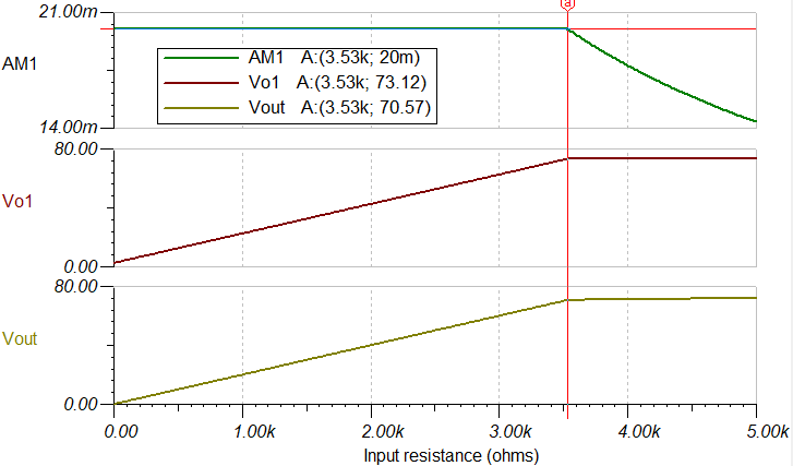
The OPA455 current pump sources or sinks a constant current through a load resistance of 0 Ω on the low end, to just beyond 4.25 kΩ on the high end. This current range is portrayed in the dc transfer plot show in Figure 8-4. As shown, the load can be vary from 0 Ω to 4.25 kΩ and the output remains within the span of linear output compliance range.
 Figure 8-4 Output Voltage Compliance for
an Improved Howland Current Pump
Figure 8-4 Output Voltage Compliance for
an Improved Howland Current PumpThe 4.25-kΩ limit is determined by the maximum 70-V drop across the load, and the 2.5-V drop across R13 when 20 mA flows through both. This voltage drop results in an output voltage of 87.5 V at the output of the OPA455, close to the positive swing limit. Beyond 4.25 kΩ, current-pump operation is forced outside the compliance range, and the output current is longer maintained at the correct level.
The OPA455 provides this wide output compliance range because of the wide, ±75-V power supply rating. If a standard ±15-V amplifier supply was used with the OPA455, or another amplifier rated for ±15-V supplies, the maximum load resistance is on the order of approximately 500 Ω to 600 Ω depending on the particular amplifier linear output range when delivering ±20 mA. The wide supply range of the OPA455 enables the device to drive a much wider range of loads.
The improved Howland current pump can also be used to generate an accurate ac current with a peak output that matches a specified dc current level. A ±20-mA dc current source using the OPA455 has already been discussed; therefore, this current source is applied here to demonstrate how a 400-Hz, 20-mA current is produced.
The same improved Howland current pump circuit used previously is updated so that the 2.5-V dc voltage source has been replaced by a 400-Hz ac source with a peak voltage of 2.5 V, as shown in Figure 8-5. A sine wave is used in this circuit, but a triangle wave, square wave, and so on, can be used instead. The output current is dependent on the ac input voltage at any particular moment.
 Figure 8-5 OPA455 Configured as a 400-Hz
AC Current Generator
Figure 8-5 OPA455 Configured as a 400-Hz
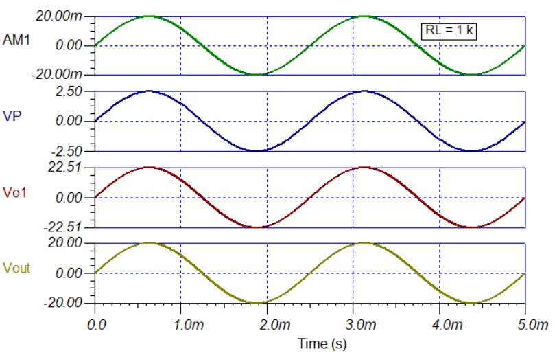
AC Current GeneratorA 2.5-Vpk sine-wave source applied to the input point at R11 results in a 20-mA peak current through the load, as shown in Figure 8-6. The load has been set to 1 kΩ, but any resistance that supports the output compliance range can be used.
 Figure 8-6 Improved Howland Current Pump
Applied as a Peak AC-Current Generator
Figure 8-6 Improved Howland Current Pump
Applied as a Peak AC-Current GeneratorMake sure to consider the power handling ratings of the resistors used with a high-power or high-voltage amplifier such as the OPA455. In this design, when the OPA455 is providing 20 mA dc to a 4.25-kΩ load resistance, the dc power for the load and R13 is simply:
- Load Power = I2 ∙ RL = (20 ∙ 10 – 3 A)2 (4.25 ∙ 103 Ω) = 1.7 W
- Power R13 = I2 ∙ R13 = (20 ∙ 10 – 3 A)2 (125 Ω) = 50 mW
Clearly, the power dissipation of the load requires attention. However, in this design, R13 does not require high power dissipation under these operating conditions. The load must be rated to dissipate the 1.7 W over the expected operating temperature range for this example. Most often, resistor power dissipation is specified at an ambient temperature of 25°C, and reduces as temperature increases. The use of a resistor with a power rating greater than the power that must be dissipated is almost always necessary. For this example, the load may need to be rated for 3 W, or even 5 W, to make sure that the load does not overheat and maintains reliability. in any case, determine the power dissipation for the particular operating conditions. Be especially attentive to the power rating issue regarding surface-mount resistors. The thermal environment in which surface-mount resistors operate may be much different than a resistor exposed in free air.
The improved Howland current pump amplifier circuit relies on both negative and positive feedback for operation. More negative feedback than positive feedback is used, but that does not always provide stability when the output load characteristics are included. When unity-gain stable amplifiers such as the OPA455 are employed, and they drive a resistive load, the amplifier phase margin should be sufficient so that the circuit is stable. However, if the output load is complex, containing both resistive and reactive components (R±jX), certain combinations degrade the phase margin to the point where instability results. Instability is even more evident when this current pump is used to drive certain inductive loads.
When required, compensation is determined based on the particular circuit to which the OPA455 is being applied. Amplifier stability and compensation is a vast subject covered in numerous TI documents, and TI training programs, such as TI Precision Labs – Op Amps.