ZHCSJ65A December   2018  – December 2019 OPA462

PRODUCTION DATA.  

  1. 特性
  2. 应用
  3. 说明
    1.     Device Images
      1.      OPA462 方框图
      2.      最大输出电压与频率间的关系
  4. 修订历史记录
  5. Pin Configuration and Functions
    1.     Pin Functions
  6. Specifications
    1. 6.1 Absolute Maximum Ratings
    2. 6.2 ESD Ratings
    3. 6.3 Recommended Operating Conditions
    4. 6.4 Thermal Information
    5. 6.5 Electrical Characteristics
    6. 6.6 Typical Characteristics: Table of Graphs
    7. 6.7 Typical Characteristics
  7. Detailed Description
    1. 7.1 Overview
    2. 7.2 Functional Block Diagram
    3. 7.3 Feature Description
      1. 7.3.1 Status Flag Pin
      2. 7.3.2 Thermal Protection
      3. 7.3.3 Current Limit
      4. 7.3.4 Enable and Disable
    4. 7.4 Device Functional Modes
  8. Application and Implementation
    1. 8.1 Application Information
    2. 8.2 Typical Applications
      1. 8.2.1 High DAC Gain Stage for Semiconductor Test Equipment
        1. 8.2.1.1 Design Requirements
        2. 8.2.1.2 Detailed Design Procedure
        3. 8.2.1.3 Application Curve
      2. 8.2.2 Improved Howland Current Pump for Bioimpedance Measurements in Multiparameter Patient Monitors
        1. 8.2.2.1 Design Requirements
        2. 8.2.2.2 Detailed Design Procedure
  9. Power Supply Recommendations
  10. 10Layout
    1. 10.1 Layout Guidelines
      1. 10.1.1 Thermally-Enhanced PowerPAD Package
      2. 10.1.2 PowerPAD Integrated Circuit Package Layout Guidelines
      3. 10.1.3 Pin Leakage
      4. 10.1.4 Thermal Protection
      5. 10.1.5 Power Dissipation
      6. 10.1.6 Heat Dissipation
    2. 10.2 Layout Example
  11. 11器件和文档支持
    1. 11.1 器件支持
      1. 11.1.1 开发支持
        1. 11.1.1.1 TINA-TI™(免费软件下载)
        2. 11.1.1.2 TI 高精度设计
        3. 11.1.1.3 WEBENCH滤波器设计器
    2. 11.2 文档支持
      1. 11.2.1 相关文档
    3. 11.3 支持资源
    4. 11.4 商标
    5. 11.5 静电放电警告
    6. 11.6 Glossary
  12. 12机械、封装和可订购信息

封装选项

机械数据 (封装 | 引脚)
散热焊盘机械数据 (封装 | 引脚)
订购信息

Heat Dissipation

Power dissipated in the OPA462 causes the junction temperature to rise. For reliable operation, junction temperature must be limited to 125°C, maximum. Maintaining a lower junction temperature always results in higher reliability. Some applications require a heat sink to make sure that the maximum operating junction temperature is not exceeded. Junction temperature can be determined according to Equation 4:

Equation 4. TJ = TA + PDRθJA

Package thermal resistance, RθJA , is affected by mounting techniques and environments. Poor air circulation and use of sockets can significantly increase thermal resistance to the ambient environment. Many op amps placed closely together also increase the surrounding temperature. Best thermal performance is achieved by soldering the op amp onto a circuit board with wide printed circuit traces to allow greater conduction through the op amp leads. Increasing circuit board copper area to approximately 0.5 in2 decreases thermal resistance; however, minimal improvement occurs beyond 0.5 in2, as shown in Figure 69.

For additional information on determining heat sink requirements, consult the Heat Sinking—TO-3 Thermal Model application bulletin, available for download at www.ti.com.
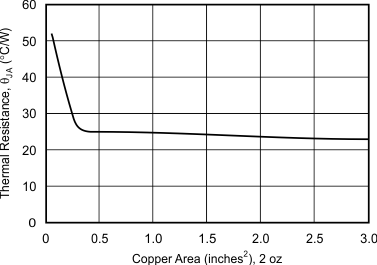
OPA462 ai_therm_res-pcb-area_bos391.gifFigure 69. Thermal Resistance vs Circuit Board Copper Area