ZHCSI51A May   2018  – June 2018 OPA521

PRODUCTION DATA.  

  1. 特性
  2. 应用
  3. 说明
    1.     Device Images
      1.      OPA521 方框图
  4. 修订历史记录
  5. Pin Configuration and Functions
    1.     Pin Functions
  6. Specifications
    1. 6.1 Absolute Maximum Ratings
    2. 6.2 ESD Ratings
    3. 6.3 Recommended Operating Conditions
    4. 6.4 Thermal Information
    5. 6.5 Electrical Characteristics
    6. 6.6 Electrical Characteristics: Digital
    7. 6.7 Electrical Characteristics: Power Supply
    8. 6.8 Typical Characteristics
  7. Detailed Description
    1. 7.1 Overview
    2. 7.2 Functional Block Diagram
    3. 7.3 Feature Description
      1. 7.3.1 IQSET Pin
      2. 7.3.2 EN Pin
      3. 7.3.3 ILIM Pin Current Limiting
      4. 7.3.4 IFLAG and TFLAG Pins
    4. 7.4 Device Functional Modes
  8. Application and Implementation
    1. 8.1 Application Information
    2. 8.2 Typical Application
      1. 8.2.1 Design Requirements
      2. 8.2.2 Detailed Design Procedure
        1. 8.2.2.1 Interfacing the OPA521 to the AC Mains
          1. 8.2.2.1.1 Low-Voltage Capacitor
          2. 8.2.2.1.2 High-Voltage Capacitor
          3. 8.2.2.1.3 Inductor
          4. 8.2.2.1.4 Line Coupling Transformer
        2. 8.2.2.2 Circuit Protection
      3. 8.2.3 Application Curves
  9. Power Supply Recommendations
  10. 10Layout
    1. 10.1 Layout Guidelines
      1. 10.1.1 Thermal Considerations
    2. 10.2 Layout Example
  11. 11器件和文档支持
    1. 11.1 器件支持
      1. 11.1.1 第三方米6体育平台手机版_好二三四免责声明
    2. 11.2 文档支持
      1. 11.2.1 相关文档
    3. 11.3 接收文档更新通知
    4. 11.4 社区资源
    5. 11.5 商标
    6. 11.6 静电放电警告
    7. 11.7 术语表
  12. 12"机械、封装和可订购信息

封装选项

机械数据 (封装 | 引脚)
散热焊盘机械数据 (封装 | 引脚)
订购信息

Typical Characteristics

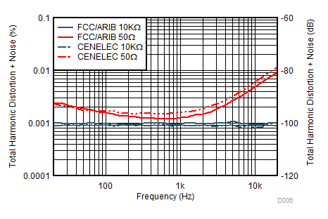
At TCASE = +25°C, V+ = 24 V, IN+ = (V+)/2, RLOAD = 50 Ω unless otherwise noted.
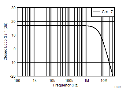
OPA521 D004_ClosedLoopGain.gif
Figure 1. Closed Loop Gain vs Frequency
OPA521 D006_THDN_Freq_7Vrms_Out_Inv.gif
VOUT = 7 VRMS
Figure 3. THD+N vs Frequency
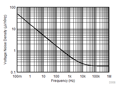
OPA521 D008_Output_Voltage_Noise.gif
Figure 5. Input Voltage Noise Spectral Density
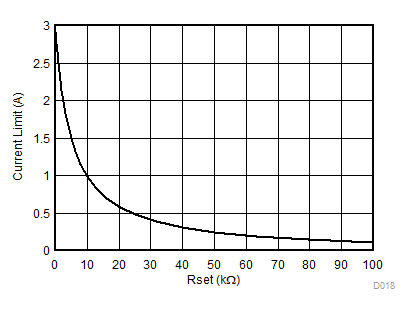
OPA521 D018_SBOS872.gif
Figure 7. Maximum Output Current Limit vs RSET
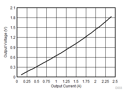
OPA521 D033_SWN_Load.gif
V+ = 15 V
Figure 9. Output Swing from GND vs Output Current (Sinking)
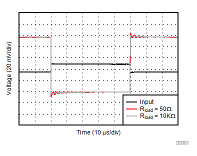
OPA521 D020_SmallSignalStep_100mV.gif
Figure 11. Small-Signal Step Response
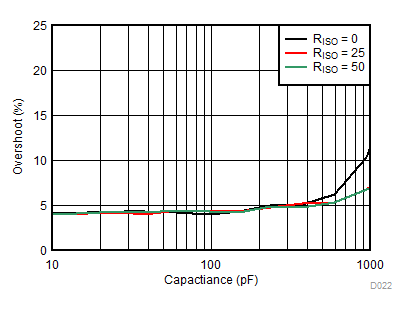
OPA521 D022_SmallSignalStep_Overshoot.gif
Figure 13. Small-Signal Overshoot vs Capacitive Load
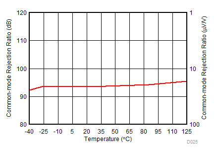
OPA521 D025CMRRvsTemp.gif
V+ = 15 V
Figure 15. CMRR vs Temperature
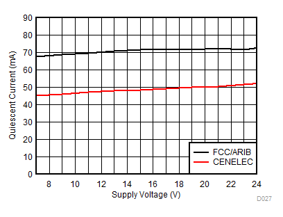
OPA521 D027_IQvsSupply.gif
V+ = 15 V
Figure 17. Iq vs Supply Voltage
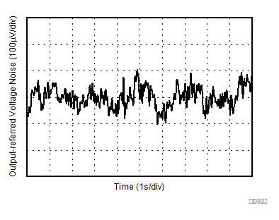
OPA521 D032_p1_10Hz_Noise.gif
Figure 19. 0.1-Hz to 10-Hz Noise
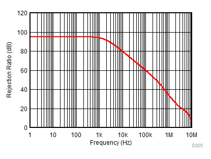
OPA521 D005_PSRR_RTI.gif
Figure 2. PSRR+ vs Frequency
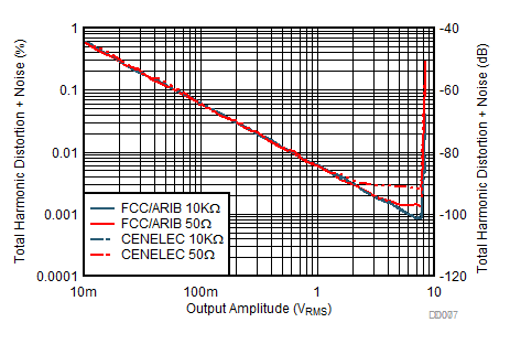
OPA521 D007_THDN_Amp_Inverting.gif
ƒ = 1 kHz
Figure 4. THD+N vs Output Amplitude
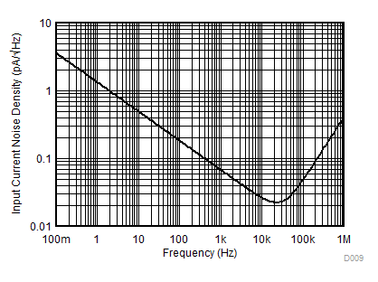
OPA521 D009_SBOS872.gif
Figure 6. Input Current Noise Density
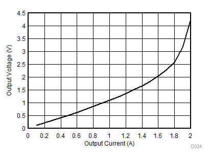
OPA521 D034_SWP_Load.gif
V+ = 15 V
Figure 8. Output Swing from V+ vs Output Current (Sourcing)
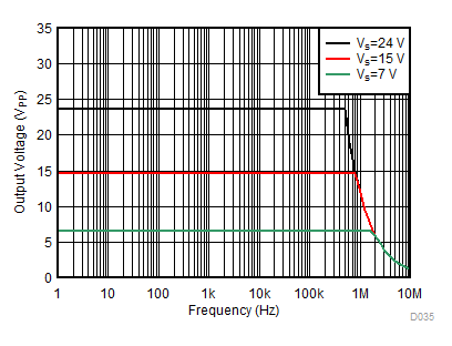
OPA521 D035_FullPowerBandwidth.gif
Figure 10. Maximum Output Voltage vs Frequency
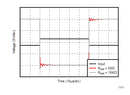
OPA521 D021_LargeSignalStep_20V.gif
Figure 12. Large-Signal Step Response
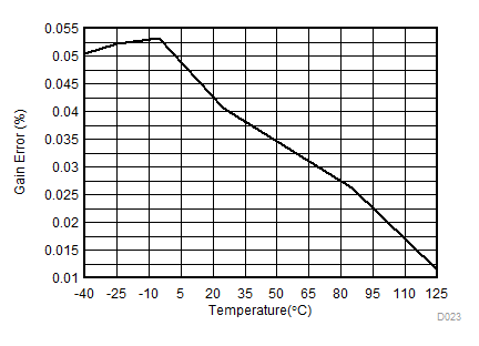
OPA521 D023gainerrorvstemp.gif
V+ = 15 V
Figure 14. Gain Error vs Temperature
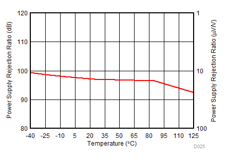
OPA521 D025PSRRvsTemp.gif
V+ = 15 V
Figure 16. PSRR vs Temperature
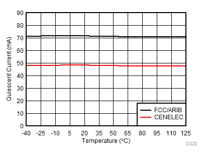
OPA521 D028_IQvsTemp12VIQHIQL.gif
V+ = 15 V
Figure 18. Iq vs Temperature