ZHCSKM1D October   1997  – December 2019 OPA548

PRODUCTION DATA.  

  1. 特性
  2. 应用
    1.     简化电路原理图
  3. 说明
  4. 修订历史记录
  5. Pin Configuration and Functions
    1.     Pin Functions
  6. Specifications
    1. 6.1 Absolute Maximum Ratings
    2. 6.2 ESD Ratings
    3. 6.3 Recommended Operating Conditions
    4. 6.4 Thermal Information
    5. 6.5 Electrical Characteristics
    6. 6.6 Typical Characteristics
  7. Detailed Description
    1. 7.1 Overview
    2. 7.2 Functional Block Diagram
    3. 7.3 Feature Description
      1. 7.3.1 Adjustable Current Limit
      2. 7.3.2 Enable/Status (E/S) Pin
      3. 7.3.3 Thermal Shutdown Status
    4. 7.4 Device Functional Modes
      1. 7.4.1 Output Disable
  8. Application and Implementation
    1. 8.1 Application Information
    2. 8.2 Typical Applications
      1. 8.2.1 Basic Circuit Connections
        1. 8.2.1.1 Design Requirements
        2. 8.2.1.2 Detailed Design Procedure
          1. 8.2.1.2.1 Power Supply Requirements
          2. 8.2.1.2.2 Gain Setting and Input Configuration
          3. 8.2.1.2.3 Current Limit
          4. 8.2.1.2.4 Safe-Operating-Area
          5. 8.2.1.2.5 Heat Sinking
        3. 8.2.1.3 Application Curve
      2. 8.2.2 Monitoring Single- and Dual-Supplies
        1. 8.2.2.1 Design Requirements
        2. 8.2.2.2 Detailed Design Procedure
          1. 8.2.2.2.1 Output Disable and Thermal Shutdown Status
      3. 8.2.3 Programmable Power Supply
    3. 8.3 System Examples
  9. Power Supply Recommendations
    1. 9.1 Output Stage Compensation
    2. 9.2 Output Protection
  10. 10Layout
    1. 10.1 Layout Guidelines
      1. 10.1.1 Safe Operating Area
      2. 10.1.2 Amplifier Mounting
      3. 10.1.3 Power Dissipation
      4. 10.1.4 Thermal Considerations
      5. 10.1.5 Heat Sinking
        1. 10.1.5.1 Heat Sink Selection Example
    2. 10.2 Layout Example
  11. 11器件和文档支持
    1. 11.1 器件支持
      1. 11.1.1 第三方米6体育平台手机版_好二三四免责声明
    2. 11.2 文档支持
      1. 11.2.1 相关文档
    3. 11.3 接收文档更新通知
    4. 11.4 支持资源
    5. 11.5 商标
    6. 11.6 静电放电警告
    7. 11.7 Glossary
  12. 12机械、封装和可订购信息

封装选项

机械数据 (封装 | 引脚)
散热焊盘机械数据 (封装 | 引脚)
订购信息

Amplifier Mounting

Figure 46 provides recommended solder footprints for both the TO-220 and DDPAK power packages. The tab of both packages is electrically connected to the negative supply, V–. It may be desirable to isolate the tab of the TO-220 package from its mounting surface with a mica (or other film) insulator (see Figure 42). For lowest overall thermal resistance it is best to isolate the entire heat sink/OPA548 structure from the mounting surface rather than to use an insulator between the semiconductor and heat sink.

For best thermal performance, the tab of the DDPAK surface-mount version should be soldered directly to a circuit board copper area. Increasing the copper area improves heat dissipation. See Figure 43 for typical thermal resistance from junction-to-ambient as a function of the copper area.
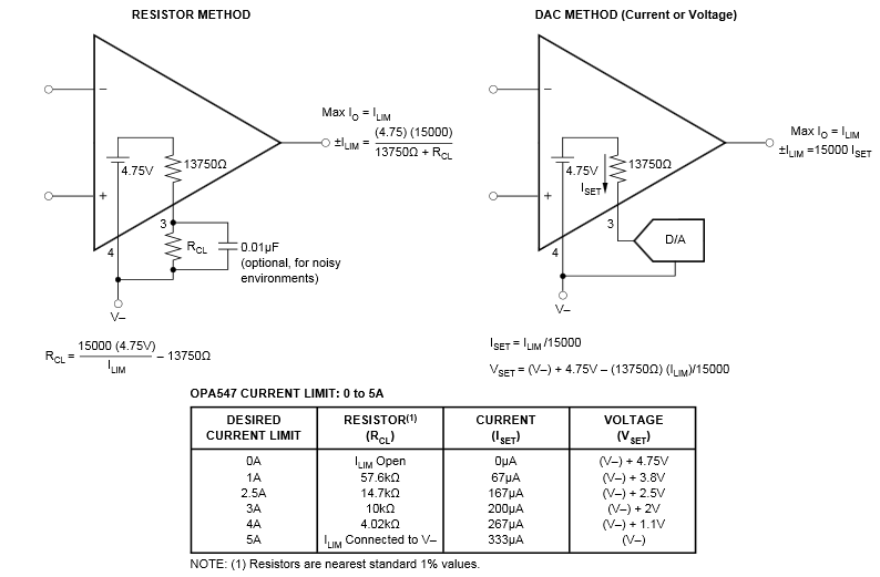
OPA548 adjcurrent.pngFigure 41. Adjustable Current Limit