ZHCS228A June 2011 – February 2024 OPA564-Q1
PRODUCTION DATA
- 1
- 1 特性
- 2 应用
- 3 说明
- 4 Device Comparison Table
- 5 Pin Configuration and Functions
- 6 Specifications
- 7 Detailed Description
- 8 Application and Implementation
- 9 Device and Documentation Support
- 10Revision History
- 11Mechanical, Packaging, and Orderable Information
5 Pin Configuration and Functions
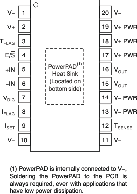
 Figure 5-1 DWP Package, 20-Pin HSOIC
(Top View)
Figure 5-1 DWP Package, 20-Pin HSOIC
(Top View)Table 5-1 Pin Functions
| PIN | TYPE | DESCRIPTION | |
|---|---|---|---|
| NAME | NO. | ||
| E/S | 4 | Input | Enable/Shutdown output stage; take E/S low to shut down output |
| IFLAG | 8 | Output | Current limit flag; active high |
| ISET | 9 | Input | Current limit set (see Section 8.1) |
| –IN | 6 | Input | Inverting op amp input |
| +IN | 5 | Input | Noninverting op amp input |
| TFLAG | 3 | Output | Thermal overtemperature flag; flag is high when alarmed and device has gone into thermal shutdown |
| TSENSE | 12 | Input/Output | Temperature sense pin for use with a remote junction temperature sensor |
| V– | 1, 10, 11, 20 | Ground | –Supply for amplifier, PWR Out, and thermal pad |
| V– PWR | 13, 14 | Ground | –Supply for power output stage |
| V+ | 2 | Power | +Supply for signal amplifier |
| V+ PWR | 17, 18, 19 | Power | +Supply for power output stage |
| VDIG | 7 | Power | +Supply for digital flag and E/S (referenced
to V–). Valid range is (V–) + 3.0V ≤ VDIG ≤ (V–) + 5.5V. |
| VOUT | 15, 16 | Output | Output voltage; RO is high impedance when shut down |
| Pad | Thermal Pad | — | Thermal pad. Connect to V– |