ZHCS228A June 2011 – February 2024 OPA564-Q1
PRODUCTION DATA
- 1
- 1 特性
- 2 应用
- 3 说明
- 4 Device Comparison Table
- 5 Pin Configuration and Functions
- 6 Specifications
- 7 Detailed Description
- 8 Application and Implementation
- 9 Device and Documentation Support
- 10Revision History
- 11Mechanical, Packaging, and Orderable Information
7.3.4 Output Shutdown
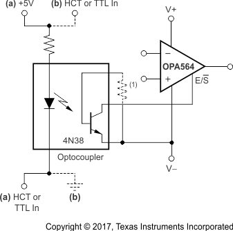
The shutdown pin (E/S) is referenced to the negative supply (V–). Therefore, shutdown operation is slightly different in single-supply and dual-supply applications. In single-supply operation, V– typically equals common ground. Therefore, the shutdown logic signal and the OPA564-Q1 shutdown pin are referenced to the same potential. In this configuration, the logic pin and the OPA564-Q1 enable can simply be connected together. Shutdown occurs for voltage levels of less than 0.8V. The OPA564-Q1 is enabled at logic levels greater than 2V. In dual-supply operation, the logic pin remains referenced to a logic ground. However, the shutdown pin of the OPA564-Q1 continues to be referenced to V–.
Thus, in a dual-supply system, to shut down the OPA564-Q1 the voltage level of the logic signal must be level-shifted by some means. One way to shift the logic signal voltage level is by using an optocoupler, as Figure 7-2 shows.

To shut down the output, the E/S pin is pulled low, no greater than 0.8V greater than V–. This function can be used to conserve power during idle periods. To return the output to an enabled state, pull the E/S pin to at least 2.0V greater than V–. Figure 6-27 shows the typical enable and shutdown response times. Be aware that the E/S pin does not affect the internal thermal shutdown.
When the OPA564-Q1 is used in applications where the device shuts down, take special care with respect to input protection. Consider the following two examples.
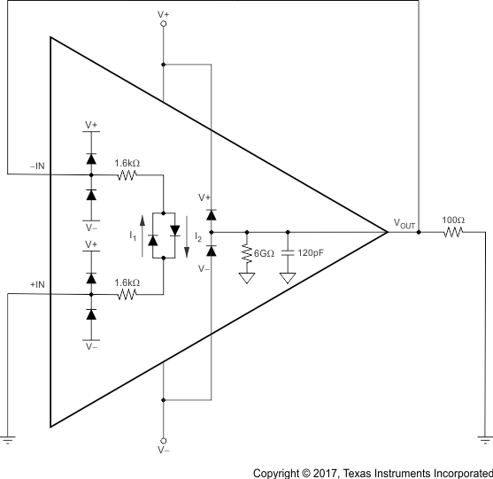
Figure 7-3 shows the amplifier in a follower configuration. The load is connected midway between the supplies, V+ and V–.
 Figure 7-3 Shutdown Equivalent Circuit
With Load Connected Midway Between Supplies
Figure 7-3 Shutdown Equivalent Circuit
With Load Connected Midway Between SuppliesWhen the device shuts down in this situation, the load pulls VOUT to ground. Little or no current then flows through the input of the OPA564-Q1.
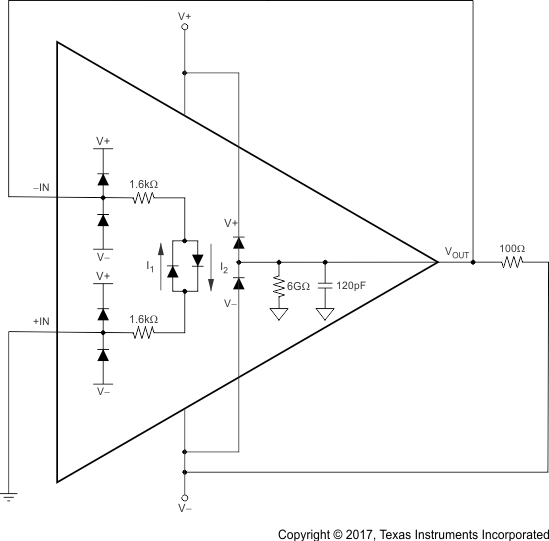
Now consider Figure 7-4. Here, the load is connected to V–. When the device shuts down, current flows from the positive input +IN through the first 1.6kΩ resistor through an input protection diode, then through the second 1.6kΩ resistor, and finally through the 100Ω resistor to V–.
This configuration damages the device.
 Figure 7-4 Shutdown Equivalent Circuit
With Load Connected to V–:
 Voltage Across Inputs During Disable Exceeds Input Requirements
This current flow produces a voltage across the inputs that is much greater than 0.5V, which damages the OPA564-Q1. A similar problem occurs if the load is connected to the positive supply.
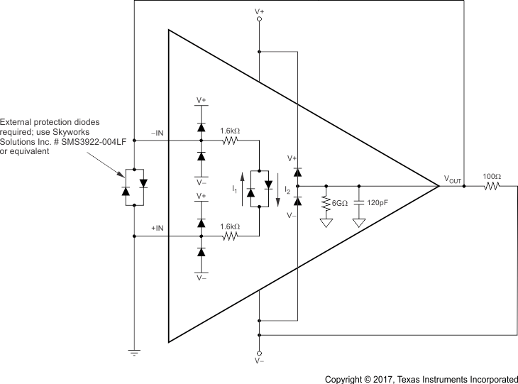
The solution is to place external protection diodes across the OPA564-Q1 input. Figure 7-5 illustrates this configuration.
This configuration protects the input during shutdown.
 Figure 7-5 Shutdown Equivalent Circuit
With Load Connected to V–: Protected Input Configuration