ZHCSDL0A April 2015 – October 2015 OPA2625 , OPA625
PRODUCTION DATA.
- 1 特性
- 2 应用
- 3 说明
- 4 修订历史记录
- 5 Pin Configuration and Functions
-
6 Specifications
- 6.1 Absolute Maximum Ratings
- 6.2 ESD Ratings
- 6.3 Recommended Operating Conditions
- 6.4 Thermal Information
- 6.5 Electrical Characteristics High-Drive Mode
- 6.6 Electrical Characteristics Low-Power Mode
- 6.7 Electrical Characteristics High-Drive Mode
- 6.8 Electrical Characteristics Low-Power Mode
- 6.9 Switching Characteristics
- 6.10 Typical Characteristics
- 7 Parameter Measurement Information
- 8 Detailed Description
- 9 Application and Implementation
- 10Power Supply Recommendations
- 11Layout
- 12器件和文档支持
- 13机械、封装和可订购信息
11 Layout
11.1 Layout Guidelines
For best operational performance of the device, use good PCB layout practices, including:
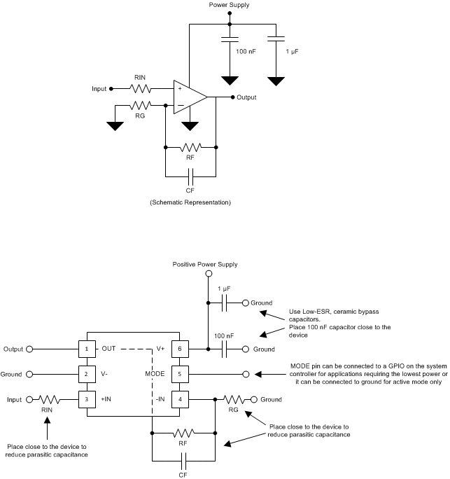
- Use bypass capacitors to reduce the noise coupled from the power supply. Connect low ESR, ceramic, bypass capacitors between the power supply pins (V+ and V–) and the ground plane. Place the bypass capacitors as close to the device as possible with the 100-nF capacitor closest to the device, as indicated in Figure 80. For single-supply applications, bypass capacitors on the V– pin are not required.
- Separate grounding for analog and digital portions of the circuitry is one of the simplest and most-effective methods of noise suppression. One or more layers on multilayer PCBs are usually devoted to ground planes. A ground plane helps distribute heat and reduces EMI noise pickup. Make sure to physically separate digital and analog grounds paying attention to the flow of the ground current. For more detailed information refer to SLOA089, Circuit Board Layout Techniques.
- In order to reduce parasitic coupling, run the input traces as far away from the supply or output traces as possible. If it is not possible to keep them separate, it is much better to cross the sensitive trace perpendicular as opposed to in parallel with the noisy trace.
- Minimize parasitic coupling between +IN and OUT for best ac performance.
- Place the external components as close to the device as possible. As shown in Figure 80, keeping RF, CF, and RG close to the inverting input will minimize parasitic capacitance.
- Keep the length of input traces as short as possible. Always remember that the input traces are the most sensitive part of the circuit.
- Cleaning the PCB following board assembly is recommended for best performance.
- Any precision integrated circuit may experience performance shifts due to moisture ingress into the plastic package. Following any aqueous PCB cleaning process, bake the PCB assembly to remove moisture introduced into the device packaging during the cleaning process. A low-temperature, post-cleaning bake at 85°C for 30 minutes is sufficient for most circumstances.
11.2 Layout Example
 Figure 80. PCB Layout Example