ZHCSTX5B September 2000 – April 2024 OPA627 , OPA637
PRODMIX
- 1
- 1 特性
- 2 应用
- 3 说明
- 4 Pin Configuration and Functions
-
5 Specifications
- 5.1 Absolute Maximum Ratings
- 5.2 ESD Ratings
- 5.3 Recommended Operating Conditions
- 5.4 Thermal Information: OPA627
- 5.5 Thermal Information: OPA637
- 5.6 Electrical Characteristics: OPA627BU, OPA627AU
- 5.7 Electrical Characteristics: OPA627AM, OPA627BM, OPA627SM
- 5.8 Electrical Characteristics: OPA637
- 5.9 Typical Characteristics
- 6 Detailed Description
- 7 Application and Implementation
- 8 Device and Documentation Support
- 9 Revision History
- 10Mechanical, Packaging, and Orderable Information
6.3.1 Offset Voltage Adjustment
The OPA6x7 are laser-trimmed for low offset voltage and drift, so many circuits do not require external adjustment. The OPA6x7 offer input offset voltage as low as ±125μV and drift as low as ±0.3μV/°C, enabling applications operating over the entire industrial temperature range.
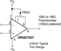
Figure 6-3 shows the optional connection of an external potentiometer to adjust offset voltage. This circuit is applicable to TO-99 packages only. Do not use this adjustment to compensate for offsets created elsewhere in a system, such as in later amplification stages or in an analog-to-digital converter (ADC).
 Figure 6-3 Optional
Offset Voltage Trim Circuit