ZHCSX79H December   2001  – October 2024 OPA690

PRODUCTION DATA  

  1.   1
  2. 特性
  3. 应用
  4. 说明
  5. Device Comparison Table
  6. Pin Configuration and Functions
  7. Specifications
    1. 6.1  Absolute Maximum Ratings
    2. 6.2  ESD Ratings
    3. 6.3  Recommended Operating Conditions
    4. 6.4  Thermal Information
    5. 6.5  Electrical Characteristics OPA690IDBV, VS = ±5 V
    6. 6.6  Electrical Characteristics OPA690IDBV, VS = 5 V
    7. 6.7  Electrical Characteristics OPA690ID, VS = ±5 V
    8. 6.8  Electrical Characteristics OPA690ID, VS = 5 V
    9. 6.9  Typical Characteristics: OPA690IDBV, VS = ±5V
    10. 6.10 Typical Characteristics: OPA690IDBV, VS = 5V
    11. 6.11 Typical Characteristics: OPA690ID, VS = ±5V
    12. 6.12 Typical Characteristics: OPA690ID, VS = 5V
  8. Detailed Description
    1. 7.1 Overview
    2. 7.2 Functional Block Diagram
    3. 7.3 Feature Description
      1. 7.3.1 Wideband Voltage-Feedback Operation
      2. 7.3.2 Input and ESD Protection
    4. 7.4 Device Functional Modes
      1. 7.4.1 Disable Operation
  9. Application and Implementation
    1. 8.1 Application Information
      1. 8.1.1 Bandwidth Versus Gain: Noninverting Operation
      2. 8.1.2 Inverting Amplifier Operation
      3. 8.1.3 Optimizing Resistor Values
      4. 8.1.4 Output Current and Voltage
      5. 8.1.5 Driving Capacitive Loads
      6. 8.1.6 Distortion Performance
      7. 8.1.7 Noise Performance
      8. 8.1.8 DC Accuracy and Offset Control
      9. 8.1.9 Thermal Analysis
    2. 8.2 Typical Applications
      1. 8.2.1 High-Performance DAC Transimpedance Amplifier
        1. 8.2.1.1 Design Requirements
        2. 8.2.1.2 Detailed Design Procedure
      2. 8.2.2 Single-Supply Active Filters
        1. 8.2.2.1 Design Requirements
        2. 8.2.2.2 Application Curve
      3. 8.2.3 High-Power Line Driver
        1. 8.2.3.1 Design Requirements
    3. 8.3 Power Supply Recommendations
    4. 8.4 Layout
      1. 8.4.1 Layout Guidelines
      2. 8.4.2 Layout Example
  10. Device and Documentation Support
    1. 9.1 Device Support
      1. 9.1.1 Macromodels and Applications Support
      2. 9.1.2 Demonstration Fixtures
    2. 9.2 接收文档更新通知
    3. 9.3 支持资源
    4. 9.4 Trademarks
    5. 9.5 静电放电警告
    6. 9.6 术语表
  11. 10Revision History
  12. 11Mechanical, Packaging, and Orderable Information

封装选项

机械数据 (封装 | 引脚)
散热焊盘机械数据 (封装 | 引脚)
订购信息

Typical Characteristics: OPA690ID, VS = ±5V

at TA = 25°C, G = 2, RF = 402Ω, and RL = 100Ω (unless otherwise noted); see Figure 7-1 for ac performance only
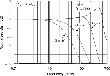
OPA690 Small-Signal Frequency Response
 
Figure 6-37 Small-Signal Frequency Response
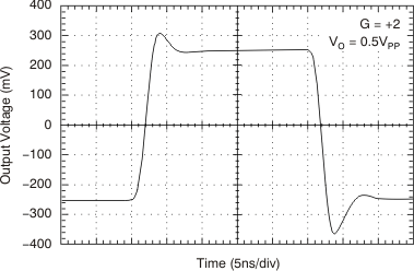
OPA690 Small-Signal Pulse Response
 
Figure 6-39 Small-Signal Pulse Response
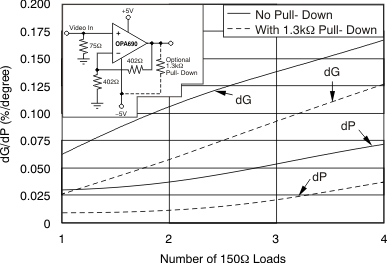
OPA690 Composite Video dG/dP
 
Figure 6-41 Composite Video dG/dP
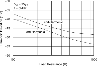
OPA690 Harmonic Distortion vs Load Resistance
 
Figure 6-43 Harmonic Distortion vs Load Resistance
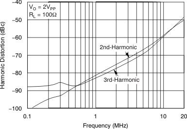
OPA690 Harmonic Distortion vs Frequency
 
Figure 6-45 Harmonic Distortion vs Frequency
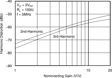
OPA690 Harmonic Distortion vs Noninverting Gain
 
Figure 6-47 Harmonic Distortion vs Noninverting Gain
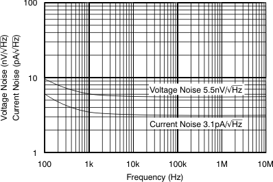
OPA690 Input
                                                Voltage and Current Noise Density
 
Figure 6-49 Input Voltage and Current Noise Density
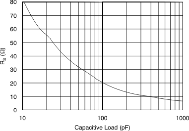
OPA690 Recommended RS vs Capacitive
                                                Load
 
Figure 6-51 Recommended RS vs Capacitive Load
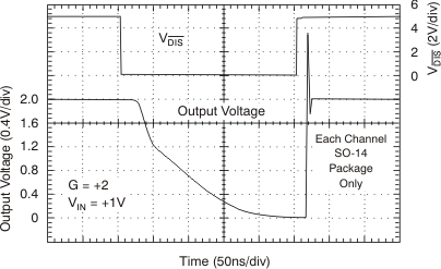
OPA690 Large-Signal Enable or Disable Response
 
Figure 6-53 Large-Signal Enable or Disable Response
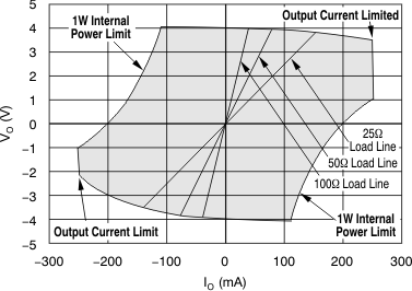
OPA690 Output Voltage and Current Limitations
 
Figure 6-55 Output Voltage and Current Limitations
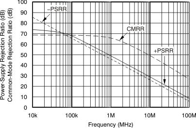
OPA690 Common−Mode Rejection Ratio and Power−Supply
                                                Rejection Ratio vs Frequency
 
Figure 6-57 Common−Mode Rejection Ratio and Power−Supply Rejection Ratio vs Frequency
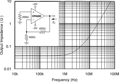
OPA690 Closed-Loop Output Impedance vs Frequency
 
Figure 6-59 Closed-Loop Output Impedance vs Frequency
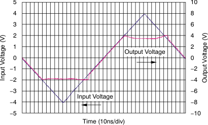
OPA690 Noninverting Overdrive Recovery
 
Figure 6-61 Noninverting Overdrive Recovery
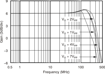
OPA690 Large-Signal Frequency Response
 
Figure 6-38 Large-Signal Frequency Response
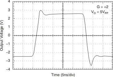
OPA690 Large-Signal Pulse Response
 
Figure 6-40 Large-Signal Pulse Response
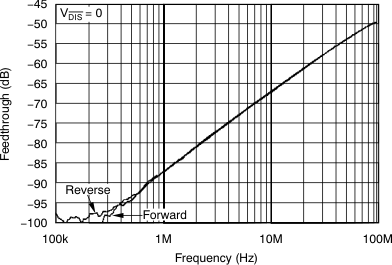
OPA690 Disable Feedthrough vs Frequency
 
Figure 6-42 Disable Feedthrough vs Frequency
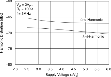
OPA690 5MHz
                                                Harmonic Distortion vs Supply Voltage
 
Figure 6-44 5MHz Harmonic Distortion vs Supply Voltage
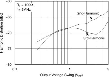
OPA690 Harmonic Distortion vs Output Voltage
 
Figure 6-46 Harmonic Distortion vs Output Voltage
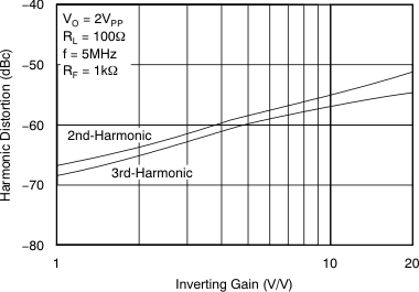
OPA690 Harmonic Distortion vs Inverting Gain
 
Figure 6-48 Harmonic Distortion vs Inverting Gain
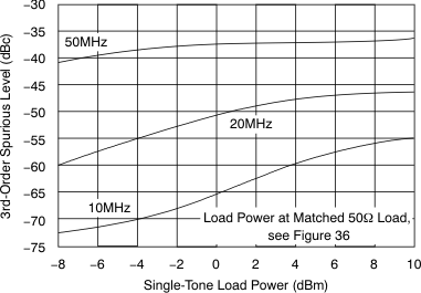
OPA690 Two-Tone, 3rd-Order Intermodulation
                                                Spurious
 
Figure 6-50 Two-Tone, 3rd-Order Intermodulation Spurious
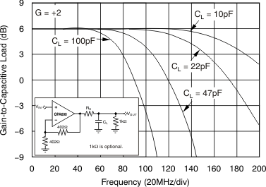
OPA690 Frequency Response vs Capacitive Load
 
Figure 6-52 Frequency Response vs Capacitive Load
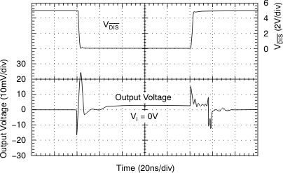
OPA690 Enable or Disable Glitch
 
Figure 6-54 Enable or Disable Glitch
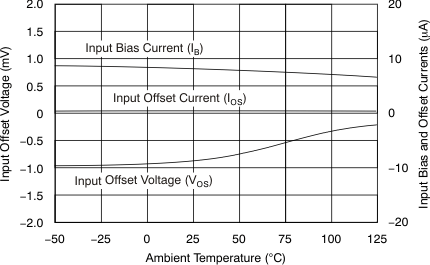
OPA690 Typical DC Drift Over Temperature
 
Figure 6-56 Typical DC Drift Over Temperature
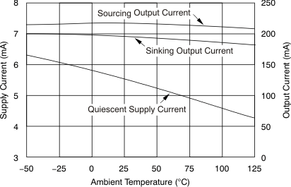
OPA690 Supply and Output Currents vs Temperature
 
Figure 6-58 Supply and Output Currents vs Temperature
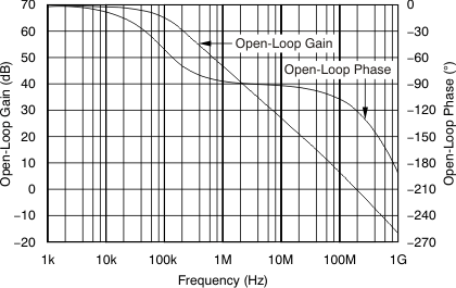
OPA690 Open−Loop Gain and Phase
 
Figure 6-60 Open−Loop Gain and Phase