ZHCSR21I December 2003 – October 2024 OPA695
PRODUCTION DATA
- 1
- 1 特性
- 2 应用
- 3 说明
- 4 Pin Configuration and Functions
-
5 Specifications
- 5.1 Absolute Maximum Ratings
- 5.2 ESD Ratings
- 5.3 Recommended Operating Conditions
- 5.4 Thermal Information
- 5.5 Electrical Characteristics VS = ±5 V, OPA695ID, OPA695IDBV
- 5.6 Electrical Characteristics VS = 5 V, OPA695ID, OPA695IDBV
- 5.7 Electrical Characteristics VS = ±5 V, OPA695IDGK
- 5.8 Electrical Characteristics VS = 5 V, OPA695IDGK
- 5.9 Typical Characteristics: VS = ±5 V, OPA695IDBV, OPA695ID
- 5.10 Typical Characteristics: VS = 5 V, OPA695IDBV, OPA695ID
- 5.11 Typical Characteristics: VS = ±5 V, OPA695IDGK
- 5.12 Typical Characteristics: VS = 5 V, OPA695IDGK
- 6 Detailed Description
- 7 Application and Implementation
- 8 Device and Documentation Support
- 9 Revision History
- 10Mechanical, Packaging, and Orderable Information
封装选项
机械数据 (封装 | 引脚)
散热焊盘机械数据 (封装 | 引脚)
订购信息
7.1.3.1 Cable Modem Return Path Driver
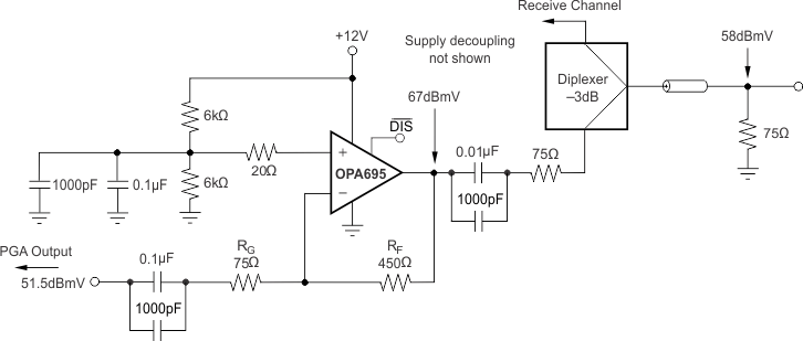
The standard cable modem upstream driver is typically required to drive high power over a 5-MHz to 65-MHz bandwidth while delivering < –50-dBc distortion. Highly-integrated solutions (including programmable gain stages) often fall short of this target as a result of high losses from the amplifier output to the line. The higher gain-operating capability of the OPA695 and the very high slew rate provide a low-cost device for delivering this signal with the required spurious-free dynamic range. Figure 7-6 shows one example of using the OPA695 as an upstream driver for a cable modem return path. In this case, the input impedance of the driver is set to 75 Ω by the gain resistor (RG). The required input level from the adjustable gain stage is significantly reduced by the 15.5-dB gain provided by the OPA695. In this example, the physical 75-Ω output matching resistor, along with the 3-dB loss in the diplexer, attenuate the output swing by 9 dB on the line. In this example, a single +12-V supply id used to achieve the lowest harmonic distortion for the 6-VPP output pin voltage through 65 MHz. Measured performance for this example gives a 600-MHz small-signal bandwidth and < –54-dBc distortion through 65 MHz for a 6-VPP output pin voltage swing.
An alternative to this circuit that gives even lower distortion is a differential driver using two OPA695 devices driving into an output transformer. The differential driver can be used to either double the available line power or improve distortion by cutting the required output swing in half for each stage. The channel disable required by the MCNS specification must be implemented by using the PGA disable feature. The MCNS disable specification requires that an output impedance match be maintained with the signal channel shut off. The disable feature of the OPA695 is intended principally for power savings and puts the output and inverting input pins into a high-impedance mode, but does not maintain the required output-impedance matching. Turning off the signal at the input of Figure 7-6, while keeping the OPA695 active, maintains the impedance matching while putting very little noise on the line. The line noise in disable for the circuit of Figure 7-6 (with the PGA source turned off, but still presenting a 75-Ω source impedance) is a very low 4 nV/√Hz (–157 dBm/Hz) as a result of the low input noise of the OPA695.
 Figure 7-6 Cable Modem Upstream Driver