ZHCSOI9A July   2022  – December 2022 OPA817

PRODUCTION DATA  

  1. 特性
  2. 应用
  3. 说明
  4. Revision History
  5. Device Comparison Table
  6. Pin Configuration and Functions
  7. Specifications
    1. 7.1 Absolute Maximum Ratings
    2. 7.2 ESD Ratings
    3. 7.3 Recommended Operating Conditions
    4. 7.4 Thermal Information
    5. 7.5 Electrical Characteristics: VS = ±5 V
    6. 7.6 Typical Characteristics: VS = ±5 V
  8. Detailed Description
    1. 8.1 Overview
    2. 8.2 Functional Block Diagram
    3. 8.3 Feature Description
      1. 8.3.1 Input and ESD Protection
      2. 8.3.2 Feedback Pin
      3. 8.3.3 FET-Input Architecture with Wide Gain-Bandwidth Product
      4. 8.3.4 Device Functional Modes
        1. 8.3.4.1 Power-Down (PD) Pin
  9. Application and Implementation
    1. 9.1 Application Information
      1. 9.1.1 Wideband, High-Input Impedance DAQ Front-End
    2. 9.2 Typical Applications
      1. 9.2.1 High Input Impedance, 200 MHz, Digitizer Front-End Amplifier Design
      2. 9.2.2 Design Requirements
      3. 9.2.3 Detailed Design Procedure
      4. 9.2.4 Application Curves
  10. 10Power Supply Recommendations
  11. 11Layout
    1. 11.1 Layout Guidelines
      1. 11.1.1 Thermal Considerations
    2. 11.2 Layout Example
  12. 12Device and Documentation Support
    1. 12.1 Device Support
      1. 12.1.1 Development Support
    2. 12.2 Documentation Support
      1. 12.2.1 Related Documentation
    3. 12.3 接收文档更新通知
    4. 12.4 支持资源
    5. 12.5 Trademarks
    6. 12.6 Electrostatic Discharge Caution
    7. 12.7 术语表
  13. 13Mechanical, Packaging, and Orderable Information

封装选项

机械数据 (封装 | 引脚)
散热焊盘机械数据 (封装 | 引脚)
订购信息

Feedback Pin

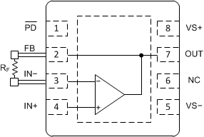
For high speed analog design, minimizing parasitic capacitances and inductances is critical to get the best performance from a high-speed amplifier such as the OPA817. Parasitic capacitance and inductance are especially detrimental in the feedback path and at the inverting input. They result in undesired poles and zeroes in the feedback that could result in reduced phase margin or instability. Techniques used to correct this phase margin reduction often result in reduced application bandwidth. To keep system engineers from making these tradeoff choices and to simplify the PCB layout, OPA817 features an FB pin on the same side as the inverting input pin (IN–). Figure 8-4 shows how this feature allows for a very short feedback resistor (RF) connection between the FB and the IN– pin, which minimizes parasitic capacitance and inductance with minimal PCB design effort. Internally the FB pin is connected to OUT pin through metal routing on the silicon. Due to the fixed metal sizing of this connection, the FB pin has limited current carrying capability. Therefore, the specifications in the Absolute Maximum Ratings section must be adhered to for continuous operation. For applications requiring high accuracy, the metal routing resistance from OUT to FB can be considered and added to RF to set the desired gain. For more information, see Section 7.5.
GUID-36F0C60E-3602-4F2B-BA27-BBE4CA366538-low.gifFigure 8-4 RF Connection Between FB and IN– Pins