SBOS303D June 2004 – December 2016 OPA820
PRODUCTION DATA.
- 1 Features
- 2 Applications
- 3 Description
- 4 Revision History
- 5 Device Comparison Table
- 6 Pin Configuration and Functions
- 7 Specifications
- 8 Parameter Measurement Information
- 9 Detailed Description
- 10Application and Implementation
- 11Power Supply Recommendations
- 12Layout
- 13Device and Documentation Support
- 14Mechanical, Packaging, and Orderable Information
封装选项
请参考 PDF 数据表获取器件具体的封装图。
机械数据 (封装 | 引脚)
- D|8
- DBV|5
散热焊盘机械数据 (封装 | 引脚)
订购信息
10 Application and Implementation
NOTE
Information in the following applications sections is not part of the TI component specification, and TI does not warrant its accuracy or completeness. TI’s customers are responsible for determining suitability of components for their purposes. Customers should validate and test their design implementation to confirm system functionality.
10.1 Application Information
10.1.1 Optimizing Resistor Values
Because the OPA820 device is a unity-gain stable, voltage-feedback op amp, a wide range of resistor values can be used for the feedback and gain-setting resistors. The primary limits on these values are set by dynamic range (noise and distortion) and parasitic capacitance considerations. Usually, the feedback resistor value is from
200 Ω to 1 kΩ. At less than 200 Ω, the feedback network presents additional output loading which can degrade the harmonic distortion performance of the OPA820 device. At greater than 1 kΩ, the typical parasitic capacitance (approximately 0.2 pF) across the feedback resistor can cause unintentional band limiting in the amplifier response. A direct short is suggested as a feedback for AV = 1 V/V.
A good design practice is to target the parallel combination of RF and RG (see Figure 55) to be less than approximately 200 Ω. The combined impedance RF || RG interacts with the inverting input capacitance, placing an additional pole in the feedback network, and thus a zero in the forward response. Assuming a total parasitic of
2 pF on the inverting node, holding RF || RG < 200 Ω keeps this pole above 400 MHz. This constraint implies that the feedback resistor RF can increase to several kΩ at high gains which is acceptable as long as the pole formed by RF and any parasitic capacitance appearing in parallel is kept out of the frequency range of interest.
In the inverting configuration, an additional design consideration must be considered. RG becomes the input resistor and therefore the load impedance to the driving source. If impedance matching is desired, RG can be set equal to the required termination value. However, at low inverting gains, the resulting feedback resistor value can present a significant load to the amplifier output. For example, an inverting gain of 2 with a 50-Ω input matching resistor (RG) requires a 100-Ω feedback resistor, which contributes to output loading in parallel with the external load. In such a case, increasing both the RF and RG values is preferable, and then achieve the input matching impedance with a third resistor to ground (see Figure 56). The total input impedance becomes the parallel combination of RG and the additional shunt resistor.
10.2 Typical Applications
10.2.1 Active Filter Design
Most active filter topologies have exceptional performance using the broad bandwidth and unity-gain stability of the OPA820 device. Topologies employing capacitive feedback require a unity-gain stable, voltage-feedback op amp. Sallen-Key filters simply use the op amp as a noninverting gain stage inside an RC network. Either current feedback or voltage-feedback op amps can be used in Sallen-Key implementations.
10.2.1.1 Design Requirements
The design requirements for the active filters are given in Table 2:
Table 2. Design Requirements
| FILTER TYPE | Q | FILTER CUTOFF FREQUENCY f-3dB (MHz) |
DC GAIN (dB) |
|---|---|---|---|
| Second order Butterworth, low-pass filter | 0.707 | 5 | 6 |
| High-Q, bandpass filter | 10 | 1 | — |
10.2.1.2 Detailed Design Procedure
10.2.1.2.1 High-Q Bandpass Filter Design Procedure
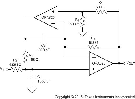
The transfer function of a high-Q bandpass filter shown in Figure 64 is given by Equation 9.


Use Equation 11 and Equation 12, along with the filter specifications in table to find the relationship between ω0, Q, R1, and C1. Set C1 = 1000 pF, which results in R1= 1.5915 kΩ. The closest E96 standard value resistor value is 1.58 kΩ.
Notice that the DC load driven by the OPA820 driving the output VOUT = R3 + R4. Select the total load to be 1 kΩ and R3 = R4, which results in a value of 500 Ω.
To simplify the filter design, set C1 = C2 = 1000 pF.
Plugging the values of R3, R4, C1, and C2 into Equation 10 and assuming R2 = R5 results in a value of 159.15 Ω. The closest standard E96 value is 158 Ω.
See Figure 61 for the frequency response of the filter shown in Figure 60.
10.2.1.2.2 Low-Pass Butterworth Filter Design Procedure
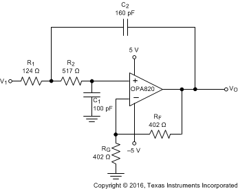
The transfer function of a low-pass Butterworth filter shown in Figure 59 is given by Equation 13.

where
-
 is the low-frequency DC gain
The values for RF and RG are the standard recommended values in the data sheet.
The cutoff frequency is in Equation 14.

The Q of the filter is given by Equation 15.

From Table 1, Q = 0.707 and ω0 = 2π × 5 MHz. To aid in solving this circuit, assume C1 = 100 pF and R1 = 124 Ω. Plugging these values into Equation 14 and Equation 15 and finding the closest standard value components results in R2 = 517 Ω and C2 = 160 pF. See Figure 62 for the frequency response of the filter shown in Figure 59.
10.2.1.3 Application Curves
 Figure 61. High-Q 1-MHz Bandpass Filter Frequency Response
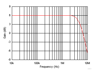 Figure 62. Frequency Response
10.2.2 Buffering High-Performance ADCs
To achieve full performance from a high-dynamic range ADC, take considerable care in the design of the input-amplifier interface circuit. The example circuit in Figure 63 shows a typical AC-coupled interface to a very-high dynamic-range converter. This AC-coupled example allows the OPA820 device to operate using a signal range that swings symmetrically around ground (0 V). The 2-VPP swing is then level-shifted through the blocking capacitor to a midscale reference level, which is created by a well-decoupled resistive divider off the internal reference voltages of the converter. To have a negligible effect (1 dB) on the rated spurious-free dynamic range (SFDR) of the converter, the SFDR of the amplifier must be at least 18 dB greater than the converter. The OPA820 device has a minimal effect on the rated distortion of the ADS850 device, given the 79-dB SFDR at 2 VPP, 1 MHz of the ADS850 device. The greater than 90-dB (<1 MHz) SFDR for the OPA820 device in this configuration implies a less than 3-dB degradation (for the system) from the specification of the converter. For additional SFDR improvement with the OPA820 device, use a differential configuration.
Successful application of the OPA820 device for ADC driving requires careful selection of the series resistor at the amplifier output and the additional shunt capacitor at the ADC input. To some extent, the selection of this RC network is determined empirically for each converter. Many high-performance CMOS ADCs, such as the ADS850, perform better with the shunt capacitor at the input pin. This capacitor provides low source impedance for the transient currents produced by the sampling process. Improved SFDR is often obtained by adding this external capacitor, whose value is often recommended in the data sheet of the converter. The external capacitor, in combination with the built-in capacitance of the ADC input, presents a significant capacitive load to the OPA820 device. Without a series isolation resistor, an undesirable peaking or loss of stability in the amplifier can occur.
Because the DC bias current of the CMOS ADC input is negligible, the resistor has no effect on overall gain or offset accuracy. See Figure 15 (±5 V) and Figure 42 (5 V) to obtain a good starting value for the series resistor which ensures a flat-frequency response to the ADC input. Increasing the external capacitor value allows the series resistor to be reduced. Intentionally band limiting using this RC network can also be used to limit noise at the converter input.
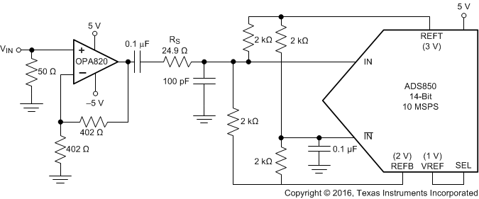 Figure 63. High Dynamic-Range Converter
10.2.3 Video Line Driving
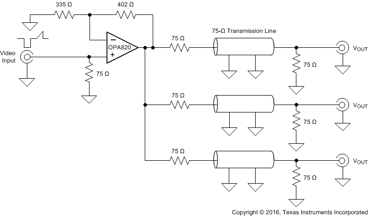
Most video distribution systems are designed with 75-Ω series resistors to drive a matched 75-Ω cable. To deliver a net gain of 1 to the 75-Ω matched load, the amplifier is typically set up for a voltage gain of 2, compensating for the 6-dB attenuation of the voltage divider formed by the series and shunt 75-Ω resistors at either end of the cable.
The circuit of Figure 55 applies to this requirement if all references to 50-Ω resistors are replaced by 75-Ω values. Often, the amplifier gain is further increased to 2.2, which recovers the additional DC loss of a typical long cable run. This change would require the gain resistor (RG) in Figure 55 to be reduced from 402 Ω to 335 Ω. In either case, both the gain flatness and the differential gain and phase performance of the OPA820 device provides exceptional results in video-distribution applications. Differential gain and phase measure the change in overall small-signal gain and phase for the color sub-carrier frequency (3.58 MHz in NTSC systems) versus changes in the large-signal output level (which represents luminance information in a composite video signal). The OPA820 device, with the typical 150-Ω load of a single-matched video cable, shows less than 0.01% differential gain and 0.01° phase errors over the standard luminance range for a positive video (negative sync) signal. Similar performance can be observed for multiple video signals, as shown in Figure 64.
10.2.4 Single Differential Op Amp
The voltage-feedback architecture of the OPA820 device, with the high common-mode rejection ratio (CMRR), provides exceptional performance in differential amplifier configurations. Figure 65 shows a typical configuration. The starting point for this design is the selection of the RF value from 200 Ω to 2 kΩ. Lower values reduce the required RG, increasing the load on the V2 source and on the OPA820 output. Higher values increase output noise as well as the effects of parasitic board and device capacitances. Following the selection of RF, RG must be set to achieve the desired inverting gain for V2. Remember that the bandwidth is set approximately by the gain bandwidth product (GBP) divided by the noise gain (1 + RF / RG). For accurate differential operation (that is, good CMRR), the ratio R2 / R1 must be set equal to RF / RG.
Usually, setting the absolute values of R2 and R1 equal to RF and RG (respectively) is best. This setting equalizes the divider resistances and cancels the effect of input bias currents. However, scaling the values of R2 and R1 to adjust the loading on the driving source, V1, can be useful. In most cases, the achievable low-frequency CMRR is limited by the accuracy of the resistor values. The 85-dB CMRR of the OPA820 device does not determine the overall circuit CMRR unless the resistor ratios are matched to better than 0.003%. If trimming the CMRR is required, R2 is the suggested adjustment point.
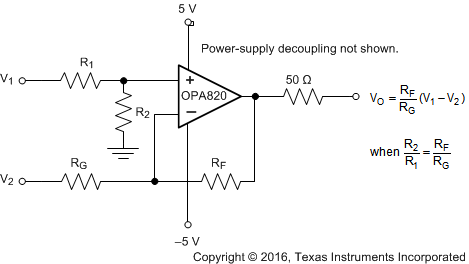 Figure 65. High-Speed, Single Differential Amplifier
10.2.5 Triple Differencing Op Amp (Instrumentation Topology)
The primary drawback of the single differential amplifier is the relatively low input impedances of the topology. Where high impedance is required at the differential input, a standard instrumentation amplifier (INA) topology can be built using the OPA820 device as the differencing stage. Figure 66 shows an example of this, in which the two input amplifiers are packaged together as a dual voltage-feedback op amp, the OPA2822 device.
This approach saves board space, cost, and power compared to using two additional OPA820 devices, and still achieves very good noise and distortion performance as a result of the moderate loading on the input amplifiers.
In this circuit, the common-mode gain to the output is always 1, because of the four matched 500-Ω resistors, whereas the differential gain is set by Equation 16 which is equal to 2 using the values in Figure 66.
The differential to single-ended conversion is still performed by the OPA820 output stage. The high-impedance inputs allow the V1 and V2 sources to be terminated or impedance-matched as required. If the V1 and V2 inputs are already truly differential, such as the output from a signal transformer, then a single-matching termination resistor can be used between them. Remember, however, that a defined DC signal path must always exist for the V1 and V2 inputs; for the transformer case, a center-tapped secondary connected to ground would provide an optimum DC operating point.
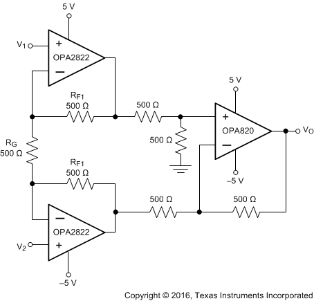 Figure 66. Wideband 3-Differencing Amplifier
10.2.6 DAC Transimpedance Amplifier
High-frequency digital-to-analog converters (DACs) require a low-distortion output amplifier to retain the SFDR performance into practical loads. Figure 67 shows a single-ended output-drive implementation. In this circuit, only one side of the complementary output drive signal is used. Figure 67 shows the signal output current connected into the virtual ground-summing junction of the OPA820 device, which is set up as a transimpedance stage or I-V converter. The unused current output of the DAC is connected to ground. If the DAC requires the outputs to be terminated to a compliance voltage other than ground for operation, then the appropriate voltage level can be applied to the noninverting input of the OPA820 device.
The DC gain for this circuit is equal to RF. At high frequencies, the DAC output capacitance (CD) produces a zero in the noise gain for the OPA820 device that can cause peaking in the closed-loop frequency response. CF is added across RF to compensate for this noise-gain peaking. To achieve a flat transimpedance-frequency response, this pole in the feedback network must be set to the value shown in Equation 17 which gives a corner frequency f–3 dB of approximately as shown in Equation 18.


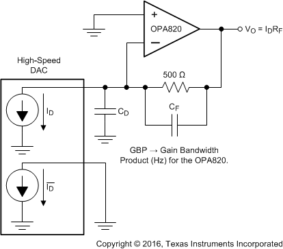 Figure 67. Wideband, Low-Distortion DAC Transimpedance Amplifier
