SBOS376I November 2006 – July 2016 OPA827
PRODUCTION DATA.
- 1 Features
- 2 Applications
- 3 Description
- 4 Revision History
- 5 Pin Configuration and Functions
- 6 Specifications
- 7 Detailed Description
- 8 Application and Implementation
- 9 Power Supply Recommendations
- 10Layout
- 11Device and Documentation Support
- 12Mechanical, Packaging, and Orderable Information
7 Detailed Description
7.1 Overview
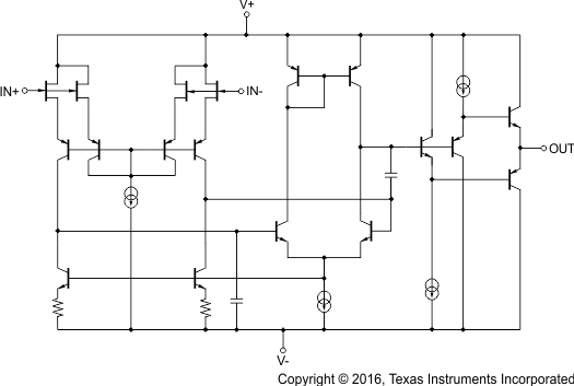
The OPA827 is a unity-gain stable, precision operational amplifier with very low noise, input bias current, and input offset voltage. Applications with noisy or high-impedance power supplies require decoupling capacitors placed close to the device pins. In most cases, 0.1-µF capacitors are adequate.
7.2 Functional Block Diagram
7.3 Feature Description
The OPA827 is a precision JFET amplifier with low input offset voltage, low input offset voltage drift and low noise. High impedance inputs make the OPA827 ideal for high source impedance applications and transimpedance applications.
7.3.1 Operating Voltage
The OPA827 series of op amps can be used with single or dual supplies from an operating range of
VS = 8 V (±4 V) and up to VS = 36 V (±18 V). This device does not require symmetrical supplies; it only requires a minimum supply voltage of 8 V. Supply voltages higher than 40 V (±20 V) can permanently damage the device; see Absolute Maximum Ratings. Key parameters are specified over the operating temperature range, TA = –40°C to 125°C. Key parameters that vary over the supply voltage or temperature range are shown in Typical Characteristics of this data sheet.
7.3.2 Noise Performance
Figure 41 shows the total circuit noise for varying source impedances with the operational amplifier in a unity-gain configuration (with no feedback resistor network and therefore no additional noise contributions). The OPA827 (GBW = 22 MHz) and OPA211 (GBW = 80 MHz) are both shown in this example with total circuit noise calculated. The op amp itself contributes both a voltage noise component and a current noise component. The voltage noise is commonly modeled as a time-varying component of the offset voltage. The current noise is modeled as the time-varying component of the input bias current and reacts with the source resistance to create a voltage component of noise. Therefore, the lowest noise op amp for a given application depends on the source impedance. For low source impedance, current noise is negligible, and voltage noise generally dominates. The OPA827 family has both low voltage noise and lower current noise because of the FET input of the op amp. Very low current noise allows for excellent noise performance with source impedances greater than 10 kΩ. OPA211 has lower voltage noise and higher current noise. The low voltage noise makes the OPA211 a better choice for low source impedances (less than 2 kΩ). For high source impedance, current noise may dominate, and makes the OPA827 series amplifier the better choice.
The equation in Figure 41 shows the calculation of the total circuit noise, with these parameters:
- en = voltage noise
- in = current noise
- RS = source impedance
- k = Boltzmann's constant = 1.38 × 10⁻²³ J/K
- T = temperature in kelvins
For more details on calculating noise, see Basic Noise Calculations.
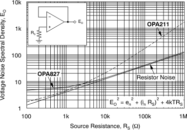 Figure 41. Noise Performance of the OPA827 and OPA211 in Unity-Gain Buffer Configuration
7.3.3 Basic Noise Calculations
Low-noise circuit design requires careful analysis of all noise sources. External noise sources can dominate in many cases; consider the effect of source resistance on the overall noise performance of the op amp. Total noise of the circuit is the root-sum-square combination of all noise components.
The resistive portion of the source impedance produces thermal noise proportional to the square root of the resistance. This function is plotted in Figure 41. The source impedance is usually fixed; consequently, select the op amp and the feedback resistors to minimize the respective contributions to the total noise.
Figure 42 illustrates both noninverting (A) and inverting (B) op amp circuit configurations with gain. In circuit configurations with gain, the feedback network resistors also contribute noise. The current noise of the op amp reacts with the feedback resistors to create additional noise components.
The feedback resistor values can generally be chosen to make these noise sources negligible.
NOTE
Low-impedance feedback resistors load the output of the amplifier. The equations for total noise are shown for both configurations shown in both configurations in Figure 42.
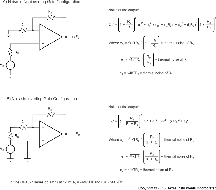 Figure 42. Noise Calculation in Gain Configurations
7.3.4 Total Harmonic Distortion Measurements
The OPA827 series op amps have excellent distortion characteristics. THD + Noise is below 0.0001%
(G = +1, VO = 3 VRMS) throughout the audio frequency range, 20 Hz to 20 kHz, with a 600-Ω load (see Figure 3).
The distortion produced by the OPA827 series is below the measurement limit of many commercially available testers. However, a special test circuit (illustrated in Figure 43) can be used to extend the measurement capabilities.
Op amp distortion can be considered an internal error source that can be referred to the input. Figure 43 shows a circuit that causes the op amp distortion to be 101 times greater than that distortion normally produced by the op amp. The addition of R3 to the otherwise standard noninverting amplifier configuration alters the feedback factor or noise gain of the circuit. The closed-loop gain is unchanged, but the feedback available for error correction is reduced by a factor of 101, thus extending the resolution by 101.
NOTE
the input signal and load applied to the op amp are the same as with conventional feedback without R3. The value of R3 must be kept small to minimize its effect on the distortion measurements.
The validity of this technique can be verified by duplicating measurements at high gain and high frequency where the distortion is within the measurement capability of the test equipment. Measurements for this data sheet were made with an Audio Precision System Two distortion and noise analyzer, which greatly simplifies such repetitive measurements. This measurement technique, however, can be performed with manual distortion measurement instruments.
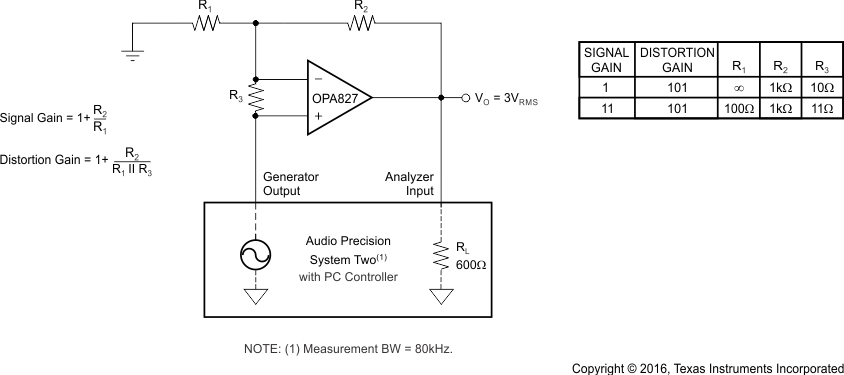 Figure 43. Distortion Test Circuit
7.3.5 Capacitive Load and Stability
The combination of gain bandwidth product (GBW) and near constant open-loop output impedance (ZO) over frequency gives the OPA827 the ability to drive large capacitive loads. Figure 44 shows the OPA827 connected in a buffer configuration (G = +1) while driving a 2.2-µF ceramic capacitor (with an ESR value of approximately 0 Ω). The small overshoot and fast settling time are results of good phase margin. This feature provides superior performance compared to the competition. Figure 44 and Figure 45 were taken without any resistive load in parallel to shorten the ringing time.
In Figure 45, the OPA827 is driving a 2.2-µF tantalum capacitor. A relatively small ESR that is internal to the capacitor additionally improves phase margin and provides an output waveform with no ringing and minimal overshoot. Figure 45 shows a stable system that can be used in almost any application.
Capacitive load drive depends on the gain and overshoot requirements of the application. Capacitive loads limit the bandwidth of the amplifier. Increasing the gain enhances the ability of the amplifier to drive greater capacitive loads (see Figure 28).
7.3.6 Phase-Reversal Protection
The OPA827 family has internal phase-reversal protection. Many FET-input op amps exhibit a phase reversal when the input is driven beyond its linear common-mode range. This condition is most often encountered in noninverting circuits when the input is driven beyond the specified common-mode voltage range, causing the output to reverse into the opposite rail. The input circuitry of the OPA827 prevents phase reversal with excessive common-mode voltage; instead, the output limits into the appropriate rail (see Figure 29).
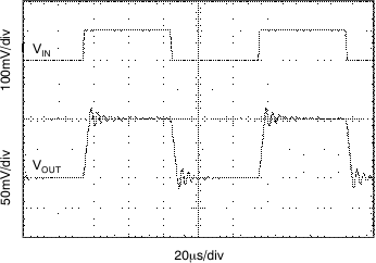 Figure 44. OPA827 Driving 2.2-µF Ceramic Capacitor
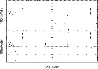 Figure 45. OPA827 Driving 2.2-µF Tantalum Capacitor
7.3.7 Transimpedance Amplifier
The gain bandwidth, low voltage noise, and current noise of the OPA827 series make them ideal wide bandwidth transimpedance amplifiers in a photo-conductive application. High transimpedance gains with feedback resistors greater than 100 kΩ benefit from the low input current noise (2.2 fA/Hz) of the JFET input. Low voltage noise is important because photodiode capacitance causes the effective noise gain in the circuit to increase at high frequencies. Total input capacitance of the circuit limits the overall gain bandwidth of the amplifier and is addressed below. Figure 46 shows a photodiode transimpedance application.
7.3.7.1 Key Transimpedance Points
- The total input capacitance (CTOT) consists of the photodiode junction capacitance, and both the common-mode and differential input capacitance of the operational amplifier.
- The desired transimpedance gain, VOUT = IDRF.
- The Unity Gain Bandwidth Product (UGBW) (22 MHz for the OPA827).
With these three variables set, the feedback capacitor value (CF) can be calculated to ensure stability. CSTRAY is the parasitic capacitance of the PCB and passive components, which is approximately 0.5 pF.
To ensure 45° phase margin, the minimal amount of feedback capacitance can be calculated using Equation 1.

Bandwidth (f–3dB) can be calculated using Equation 2.

These equations result in maximum transimpedance bandwidth. For additional information, refer to Compensate Transimpedance Amplifiers Intuitively, available for download at www.ti.com.
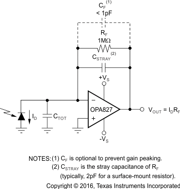 Figure 46. Transimpedance Amplifier
 Figure 47. Equivalent Schematic (Single-Channel)
7.4 Device Functional Modes
The OPA827 has a single functional mode and is operational when the power-supply voltage is greater than 4 V (±2 V). The maximum power supply voltage for the OPA827 is 36 V (±18 V).