ZHCS020J January 2011 – March 2021 OPA2835 , OPA835
PRODUCTION DATA
- 1 特性
- 2 应用
- 3 说明
- 4 Revision History
- 5 Device Comparision Table
- 6 Pin Configuration and Functions
-
7 Specifications
- 7.1 Absolute Maximum Ratings
- 7.2 ESD Ratings
- 7.3 Recommended Operating Conditions
- 7.4 Thermal Information: OPA835
- 7.5 Thermal Information: OPA2835
- 7.6 Electrical Characteristics: VS = 2.7 V
- 7.7 Electrical Characteristics: VS = 5 V
- 7.8 Typical Characteristics: VS = 2.7 V
- 7.9 Typical Characteristics: VS = 5 V
- 8 Detailed Description
-
9 Application and Implementation
- 9.1
Application Information
- 9.1.1 Noninverting Amplifier
- 9.1.2 Inverting Amplifier
- 9.1.3 Instrumentation Amplifier
- 9.1.4 Attenuators
- 9.1.5 Single-Ended to Differential Amplifier
- 9.1.6 Differential to Single-Ended Amplifier
- 9.1.7 Differential-to-Differential Amplifier
- 9.1.8 Gain Setting With OPA835 RUN Integrated Resistors
- 9.1.9 Pulse Application With Single-Supply
- 9.1.10 ADC Driver Performance
- 9.2 Typical Application
- 9.1
Application Information
- 10Power Supply Recommendations
- 11Layout
- 12Device and Documentation Support
- 13Mechanical, Packaging, and Orderable Information
封装选项
机械数据 (封装 | 引脚)
散热焊盘机械数据 (封装 | 引脚)
- RUN|10
订购信息
9.1.10 ADC Driver Performance
The OPA835 device provides excellent performance when driving high-performance delta-sigma (ΔΣ) and successive-approximation-register (SAR) ADCs in low-power audio and industrial applications.
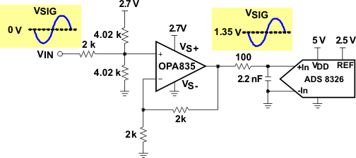
To show achievable performance, the OPA835 device is tested as the drive amplifier for the ADS8326 device. The ADS8326 device is a 16-bit, micro power, SAR ADC with pseudodifferential inputs and sample rates up to
250 kSPS. The device offers excellent noise and distortion performance in a small 8-pin SOIC or VSSOP (MSOP) package. Low power and small size make the ADS8326 and OPA835 devices an ideal solution for portable and battery-operated systems, remote data-acquisition modules, simultaneous multichannel systems, and isolated data acquisition.
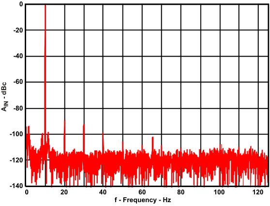
With the circuit shown in Figure 9-9 to test the performance, Figure 9-10 shows the spectral performance with a 10-kHz input frequency. The tabulated AC results are in Table 9-3.
 Figure 9-9 OPA835 and ADS8326 Test Circuit
 Figure 9-10 ADS8326 and OPA835 10-kHz FFT
| TONE (Hz) | SIGNAL (dBFS) | SNR (dBc) | THD (dBc) | SINAD (dBc) | SFDR (dBc) |
|---|---|---|---|---|---|
| 10k | –0.85 | 81.9 | –87.5 | 80.8 | 89.9 |