ZHCS019J January 2011 – March 2021 OPA2836 , OPA836
PRODUCTION DATA
- 1 特性
- 2 应用
- 3 说明
- 4 Revision History
- 5 Device Comparison Table
- 6 Pin Configuration and Functions
-
7 Specifications
- 7.1 Absolute Maximum Ratings
- 7.2 ESD Ratings
- 7.3 Recommended Operating Conditions
- 7.4 Thermal Information: OPA836
- 7.5 Thermal Information: OPA2836
- 7.6 Electrical Characteristics: VS = 2.7 V
- 7.7 Electrical Characteristics: VS = 5 V
- 7.8 Typical Characteristics: VS = 2.7 V
- 7.9 Typical Characteristics: VS = 5 V
- 8 Detailed Description
-
9 Application and Implementation
- 9.1
Application Information
- 9.1.1 Noninverting Amplifier
- 9.1.2 Inverting Amplifier
- 9.1.3 Instrumentation Amplifier
- 9.1.4 Attenuators
- 9.1.5 Single-Ended-to-Differential Amplifier
- 9.1.6 Differential-to-Signal-Ended Amplifier
- 9.1.7 Differential-to-Differential Amplifier
- 9.1.8 Gain Setting With OPA836 RUN Integrated Resistors
- 9.1.9 Pulse Application With Single-Supply
- 9.1.10 ADC Driver Performance
- 9.2 Typical Applications
- 9.1
Application Information
- 10Power Supply Recommendations
- 11Layout
- 12Device and Documentation Support
- 13Mechanical, Packaging, and Orderable Information
封装选项
机械数据 (封装 | 引脚)
散热焊盘机械数据 (封装 | 引脚)
- RUN|10
订购信息
9.2.1.3 Application Curves
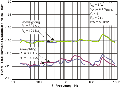
Figure 9-12 shows the THD+N performance with 100-kΩ and 300-Ω loads, and with A-weighting and with no weighting. Both loads show similar performance. With no weighting, the THD+N performance is dominated by the noise for both loads. A-weighting provides filtering that improves the noise, revealing the increased distortion with RL = 300 Ω.
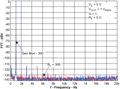
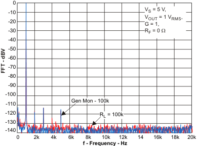
Figure 9-13 and Figure 9-14 show the FFT output with a 1-kHz tone and 100-kΩ and 300-Ω loads. To show relative performance of the device versus the test set, one channel has the OPA836 device in-line between the generator output and the analyzer. The other channel is in “Gen Mon” loopback mode, which internally connects the signal generator to the analyzer input. With 100-kΩ load, Figure 9-13, the curves are indistinguishable from each other except for noise, which means the OPA836 device cannot be directly measured. With 300-Ω load, as shown in Figure 9-14, the main difference between the curves is that the OPA836 device shows slightly higher even-order harmonics, but the performance of the test set masks the odd-order harmonics.
 Figure 9-12 OPA836 1 VRMS 20-Hz to 80-kHz THD+N
 Figure 9-14 OPA836 and AP Gen Mon 10-kHz FFT Plot; VOUT = 1 VRMS, RL = 300 Ω
 Figure 9-13 OPA836 and AP Gen Mon 10-kHz FFT Plot; VOUT = 1 VRMS, RL = 100 kΩ