ZHCS019J January 2011 – March 2021 OPA2836 , OPA836
PRODUCTION DATA
- 1 特性
- 2 应用
- 3 说明
- 4 Revision History
- 5 Device Comparison Table
- 6 Pin Configuration and Functions
-
7 Specifications
- 7.1 Absolute Maximum Ratings
- 7.2 ESD Ratings
- 7.3 Recommended Operating Conditions
- 7.4 Thermal Information: OPA836
- 7.5 Thermal Information: OPA2836
- 7.6 Electrical Characteristics: VS = 2.7 V
- 7.7 Electrical Characteristics: VS = 5 V
- 7.8 Typical Characteristics: VS = 2.7 V
- 7.9 Typical Characteristics: VS = 5 V
- 8 Detailed Description
-
9 Application and Implementation
- 9.1
Application Information
- 9.1.1 Noninverting Amplifier
- 9.1.2 Inverting Amplifier
- 9.1.3 Instrumentation Amplifier
- 9.1.4 Attenuators
- 9.1.5 Single-Ended-to-Differential Amplifier
- 9.1.6 Differential-to-Signal-Ended Amplifier
- 9.1.7 Differential-to-Differential Amplifier
- 9.1.8 Gain Setting With OPA836 RUN Integrated Resistors
- 9.1.9 Pulse Application With Single-Supply
- 9.1.10 ADC Driver Performance
- 9.2 Typical Applications
- 9.1
Application Information
- 10Power Supply Recommendations
- 11Layout
- 12Device and Documentation Support
- 13Mechanical, Packaging, and Orderable Information
封装选项
机械数据 (封装 | 引脚)
散热焊盘机械数据 (封装 | 引脚)
- RUN|10
订购信息
9.1.8 Gain Setting With OPA836 RUN Integrated Resistors
The OPA836 RUN package option includes integrated gain-setting resistors for smallest possible footprint on a printed circuit board (≈ 2.00 mm × 2.00 mm). By adding circuit traces on the PCB, gains of +1, –1, –1.33, +2, +2.33, –3, +4, –4, +5, –5.33, +6.33, –7, +8 and inverting attenuations of –0.1429, –0.1875, –0.25, –0.33, –0.75 can be achieved.
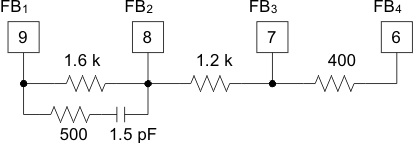
Figure 9-6 shows a simplified view of how the OPA836IRUN integrated gain-setting network is implemented. Table 9-1 lists the required pin connections for various noninverting and inverting gains (reference Figure 8-1 and Figure 8-2). Table 9-2 shows the required pin connections for various attenuations using the inverting-amplifier architecture (reference Figure 8-2). Due to ESD protection devices being used on all pins, the absolute maximum and minimum input-voltage range, VS– – 0.7 V to VS+ + 0.7 V, applies to the gain-setting resistors, so attenuation of large input voltages requires external resistors to implement.
The gain-setting resistors are laser trimmed to 1% tolerance with nominal values of 1.6 kΩ, 1.2 kΩ, and 400 Ω. The gain-setting resistors have excellent temperature coefficients, and gain drift is superior to the drift with external gain-setting resistors. The 500-Ω and 1.5-pF capacitor in parallel with the 1.6-kΩ gain-setting resistor provide compensation for best stability and pulse response.
 Figure 9-6 OPA836IRUN Gain-Setting Network
| NONINVERTING
GAIN (Figure 8-1) |
INVERTING
GAIN (Figure 8-2) |
SHORT PINS | SHORT PINS | SHORT PINS | SHORT PINS |
|---|---|---|---|---|---|
| 1 V/V (0 dB) | — | 1 to 9 | — | ||
| 2 V/V (6.02 dB) | –1 V/V (0 dB) | 1 to 9 | 2 to 8 | 6 to GND | — |
| 2.33 V/V (7.36 dB) | –1.33 V/V (2.5 dB) | 1 to 9 | 2 to 8 | 7 to GND | — |
| 4 V/V (12.04 dB) | –3 V/V (9.54 dB) | 1 to 8 | 2 to 7 | 6 to GND | — |
| 5 V/V (13.98 dB) | –4 V/V (12.04 dB) | 1 to 9 | 2 to 7 or 8 | 7 to 8 | 6 to GND |
| 6.33 V/V (16.03 dB) | –5.33 V/V (14.54 dB) | 1 to 9 | 2 to 6 or 8 | 6 to 8 | 7 to GND |
| 8 V/V (18.06 dB) | –7 V/V (16.90 dB) | 1 to 9 | 2 to 7 | 6 to GND | — |
| INVERTING
GAIN (Figure 8-2) |
SHORT PINS | SHORT PINS | SHORT PINS | SHORT PINS |
|---|---|---|---|---|
| –0.75 V/V (–2.5 dB) | 1 to 7 | 2 to 8 | 9 to GND | — |
| –0.333 V/V (–9.54 dB) | 1 to 6 | 2 to 7 | 8 to GND | — |
| –0.25 V/V (–12.04 dB) | 1 to 6 | 2 to 7 or 8 | 7 to 8 | 9 to GND |
| –0.1875 V/V (–14.54 dB) | 1 to 7 | 2 to 6 or 8 | 6 to 8 | 9 to GND |
| –0.1429 V/V (–16.90 dB) | 1 to 6 | 2 to 7 | 9 to GND | — |