ZHCSGP3D September   2017  – December 2018 OPA2837 , OPA837

PRODUCTION DATA.  

  1. 特性
  2. 应用
    1.     具有真正接地输入和输出范围的低功耗、低噪声、精密单端 SAR ADC 驱动器
  3. 说明
    1.     Device Images
  4. 修订历史记录
  5. Pin Configuration and Functions
    1.     Pin Functions
  6. Specifications
    1. 6.1  Absolute Maximum Ratings
    2. 6.2  ESD Ratings
    3. 6.3  Recommended Operating Conditions
    4. 6.4  Thermal Information: OPA837
    5. 6.5  Thermal Information: OPA2837
    6. 6.6  Electrical Characteristics: VS = 5 V
    7. 6.7  Electrical Characteristics: VS = 3 V
    8. 6.8  Typical Characteristics: VS = 5.0 V
    9. 6.9  Typical Characteristics: VS = 3.0 V
    10. 6.10 Typical Characteristics: ±2.5-V to ±1.5-V Split Supply
  7. Detailed Description
    1. 7.1 Overview
    2. 7.2 Functional Block Diagrams
    3. 7.3 Feature Description
      1. 7.3.1 OPA837 Comparison
      2. 7.3.2 Input Common-Mode Voltage Range
      3. 7.3.3 Output Voltage Range
      4. 7.3.4 Power-Down Operation
      5. 7.3.5 Low-Power Applications and the Effects of Resistor Values on Bandwidth
      6. 7.3.6 Driving Capacitive Loads
    4. 7.4 Device Functional Modes
      1. 7.4.1 Split-Supply Operation (±1.35 V to ±2.7 V)
      2. 7.4.2 Single-Supply Operation (2.7 V to 5.4 V)
  8. Application and Implementation
    1. 8.1 Application Information
      1. 8.1.1  Noninverting Amplifier
      2. 8.1.2  Inverting Amplifier
      3. 8.1.3  Output DC Error Calculations
      4. 8.1.4  Output Noise Calculations
      5. 8.1.5  Instrumentation Amplifier
      6. 8.1.6  Attenuators
      7. 8.1.7  Differential to Single-Ended Amplifier
      8. 8.1.8  Differential-to-Differential Amplifier
      9. 8.1.9  Pulse Application With Single-Supply Circuit
      10. 8.1.10 ADC Driver Performance
    2. 8.2 Typical Applications
      1. 8.2.1 Active Filters
        1. 8.2.1.1 Design Requirements
        2. 8.2.1.2 Detailed Design Procedure
        3. 8.2.1.3 Application Curves
      2. 8.2.2 Implementing a 2:1 Active Multiplexer
        1. 8.2.2.1 Design Requirements
        2. 8.2.2.2 Detailed Design Procedure
      3. 8.2.3 1-Bit PGA Operation
        1. 8.2.3.1 Design Requirements
        2. 8.2.3.2 Detailed Design Procedure
  9. Power Supply Recommendations
  10. 10Layout
    1. 10.1 Layout Guidelines
    2. 10.2 Layout Example
  11. 11器件和文档支持
    1. 11.1 文档支持
      1. 11.1.1 相关文档
    2. 11.2 相关链接
    3. 11.3 接收文档更新通知
    4. 11.4 社区资源
    5. 11.5 商标
    6. 11.6 静电放电警告
    7. 11.7 术语表
  12. 12机械、封装和可订购信息

封装选项

机械数据 (封装 | 引脚)
散热焊盘机械数据 (封装 | 引脚)
订购信息

Typical Characteristics: ±2.5-V to ±1.5-V Split Supply

with PD = VCC and TA ≈ 25°C (unless otherwise noted)
OPA837 OPA2837 D037_SBOS673.gif
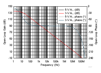
No load simulation
Figure 37. Open-Loop Gain and Phase vs Frequency
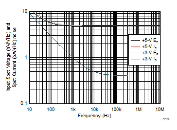
OPA837 OPA2837 D039_SBOS673.gif
Measured then fit to ideal 1/f model
Figure 39. Input Spot Noise Density vs Frequency
OPA837 OPA2837 D041_SBOS673.gif
Simulated curves
Figure 41. CMRR and PSRR vs Frequency
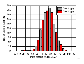
OPA837 OPA2837 D043_SBOS673.gif
830 units at each supply voltage
Figure 43. Input Offset Voltage Distribution
OPA837 OPA2837 D045_SBOS673.gif
50 units at 5-V and 3-V supply
Figure 45. Input Offset Voltage vs Ambient Temperature
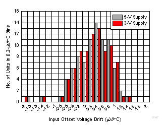
OPA837 OPA2837 D047_SBOS673.gif
–40°C to +125°C fit, 82 units, DBV package
Figure 47. Input Offset Voltage Drift Distribution
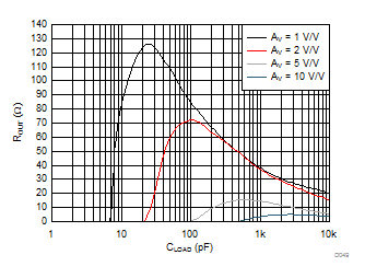
OPA837 OPA2837 D049_SBOS673.gif
See Figure 66 and Table 2, small signal,
targeting 30° phase margin
Figure 49. Output Resistor vs CLOAD
OPA837 OPA2837 D051_SBOS673.gif
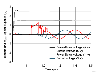
Figure 51. Turn-On Time to Sinusoidal Input
OPA837 OPA2837 D053_SBOS673.gif
Figure 53. Gain of 1 Turn-On Time to Final DC Value at Midscale (Simulated)
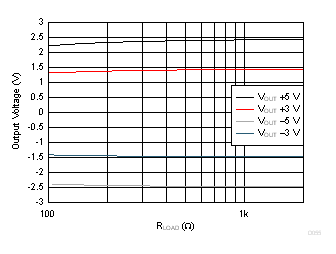
OPA837 OPA2837 D055_SBOS673.gif
Figure 55. Output Voltage Swing vs Load Resistor
OPA837 OPA2837 D057_SBOS673.gif
50 units at 5-V and 3-V supply
Figure 57. Supply Current vs Ambient Temperature
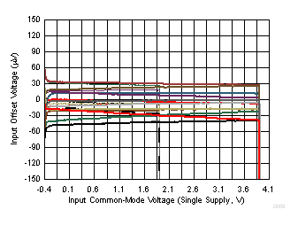
OPA837 OPA2837 D059_SBOS673.gif
12 units, 5-V and 3-V supplies
Figure 59. Input Offset Voltage vs
Input Common-Mode Voltage
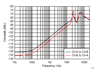
OPA837 OPA2837 D061_SBOS673.gif
Crosstalk for the OPA2837 only
Figure 61. Crosstalk vs Frequency
OPA837 OPA2837 D038_SBOS673.gif
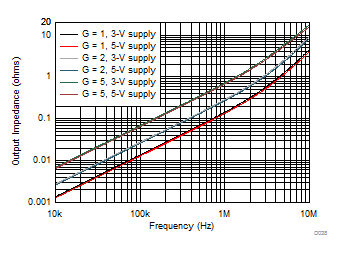
Figure 74 and Table 2 (simulation)
Figure 38. Closed-Loop Output Impedance vs Frequency
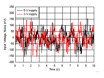
OPA837 OPA2837 D040_SBOS673.gif
Input-referred voltage noise RS = 0 Ω
Figure 40. Low-Frequency Voltage Noise vs Time
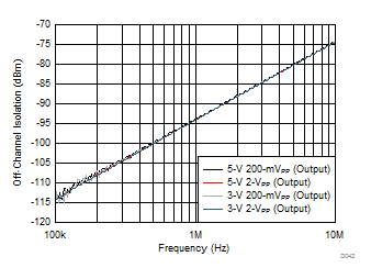
OPA837 OPA2837 D042_SBOS673.gif
Figure 42. Disabled Isolation Noninverting Input to Output vs Frequency
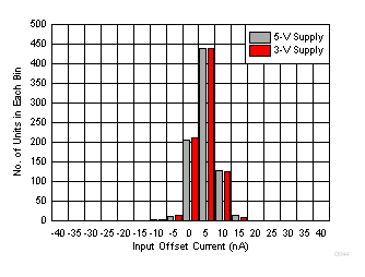
OPA837 OPA2837 D044_SBOS673.gif
830 units at each supply voltage
Figure 44. Input Offset Current Distribution
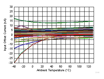
OPA837 OPA2837 D046_SBOS673.gif
50 units at 5-V and 3-V supply
Figure 46. Input Offset Current vs Ambient Temperature
OPA837 OPA2837 D048_SBOS673.gif
–40°C to +125°C fit, 82 units, DBV package
Figure 48. Input Offset Current Drift Distribution
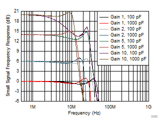
OPA837 OPA2837 D050_SBOS673.gif
Figure 50. Small-Signal Frequency Response vs CLOAD
With Recommended ROUT
OPA837 OPA2837 D052_SBOS673.gif
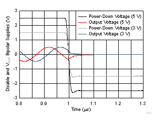
Figure 52. Turn-Off Time to Sinusoidal Input
OPA837 OPA2837 D054_SBOS673.gif
Figure 54. Gain of 2 Turn-On Time to Final DC Value at Midscale (Simulated)
OPA837 OPA2837 D056_SBOS673.gif
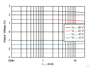
Figure 56. Output Saturation Voltage vs Load Current
OPA837 OPA2837 D058_SBOS673.gif
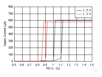
Figure 58. Supply Current vs Power-Down Voltage
(Turn-On Higher Than Turn-Off)
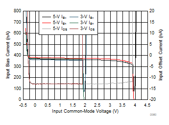
OPA837 OPA2837 D060_SBOS673.gif
Measured single device, 5-V and 3-V supplies
Figure 60. Input Bias and Offset Current vs VICM