ZHCSGP3D September 2017 – December 2018 OPA2837 , OPA837
PRODUCTION DATA.
- 1 特性
- 2 应用
- 3 说明
- 4 修订历史记录
- 5 Pin Configuration and Functions
-
6 Specifications
- 6.1 Absolute Maximum Ratings
- 6.2 ESD Ratings
- 6.3 Recommended Operating Conditions
- 6.4 Thermal Information: OPA837
- 6.5 Thermal Information: OPA2837
- 6.6 Electrical Characteristics: VS = 5 V
- 6.7 Electrical Characteristics: VS = 3 V
- 6.8 Typical Characteristics: VS = 5.0 V
- 6.9 Typical Characteristics: VS = 3.0 V
- 6.10 Typical Characteristics: ±2.5-V to ±1.5-V Split Supply
- 7 Detailed Description
-
8 Application and Implementation
- 8.1
Application Information
- 8.1.1 Noninverting Amplifier
- 8.1.2 Inverting Amplifier
- 8.1.3 Output DC Error Calculations
- 8.1.4 Output Noise Calculations
- 8.1.5 Instrumentation Amplifier
- 8.1.6 Attenuators
- 8.1.7 Differential to Single-Ended Amplifier
- 8.1.8 Differential-to-Differential Amplifier
- 8.1.9 Pulse Application With Single-Supply Circuit
- 8.1.10 ADC Driver Performance
- 8.2 Typical Applications
- 8.1
Application Information
- 9 Power Supply Recommendations
- 10Layout
- 11器件和文档支持
- 12机械、封装和可订购信息
8.1.9 Pulse Application With Single-Supply Circuit
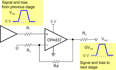
For pulsed applications where the signal is at ground and pulses to a positive or negative voltage, the circuit bias-voltage considerations differ from those in an application with a signal that swings symmetrically around a reference point. Figure 80 shows a circuit where the signal is at ground (0 V) and pulses to a positive value. The waveforms are shown slightly above ground because the output stage requires approximately 100 mV headroom to the supplies. To operate with the I/O swing truly to ground on a single-supply setup, consider using the fixed –0.23-V output LM7705.
 Figure 80. Noninverting Single-Supply Circuit With Pulse
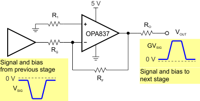
 As shown in Figure 81, an inverting amplifier is more appropriate if the input signal pulses negative from ground. A key consideration in noninverting and inverting cases is that the input and output voltages are kept within the limits of the amplifier. Because the VICR of the OPA837 includes the negative supply rail, the OPA837 op amp is well-suited for this application.
 Figure 81. Inverting Single-Supply Circuit With Pulse