ZHCSGM4D August 2017 – September 2024 OPA838
PRODMIX
- 1
- 1 特性
- 2 应用
- 3 说明
- 4 Device Comparison Table
- 5 Pin Configuration and Functions
-
6 Specifications
- 6.1 Absolute Maximum Ratings
- 6.2 ESD Ratings
- 6.3 Recommended Operating Conditions
- 6.4 Thermal Information
- 6.5 Electrical Characteristics VS = 5 V
- 6.6 Electrical Characteristics VS = 3 V
- 6.7 Typical Characteristics: VS = 5 V
- 6.8 Typical Characteristics: VS = 3 V
- 6.9 Typical Characteristics: Over Supply Range
- 7 Detailed Description
- 8 Application and Implementation
- 9 Device and Documentation Support
- 10Revision History
- 11Mechanical, Packaging, and Orderable Information
封装选项
机械数据 (封装 | 引脚)
散热焊盘机械数据 (封装 | 引脚)
订购信息
7.4.1 Split-Supply Operation (±1.35 V to ±2.7 V)
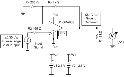
To facilitate testing with common lab equipment, the OPA838 EVM (see EVM board link) is built to allow split-supply operation. This configuration eases lab testing because the midpoint between the power rails is ground, and most signal generators, network analyzers, oscilloscopes, spectrum analyzers, and other lab equipment have inputs and outputs with a ground reference. This simplifies characterization by removing the requirement for blocking capacitors.
Figure 7-8 shows a simple noninverting configuration analogous to Figure 7-1 with a ±2.5‑V supply and VREF equal to ground. The input and output swing symmetrically around ground. For ease of use, split-supplies are preferred in systems where signals swing around ground. Using bipolar (or split) supplies shifts the thresholds for the shutdown control. The disable control is referenced from the negative supply, typically ground, in a single-supply application. However, to disable using a negative supply requires that the pin is set to within 0.55 V greater than the negative supply. If disable is not required, connect that pin to the positive supply to maintain correct operation, even for split-supply applications. Do not float the disable pin; assert the pin to a voltage.
 Figure 7-8 Split-Supply Operation
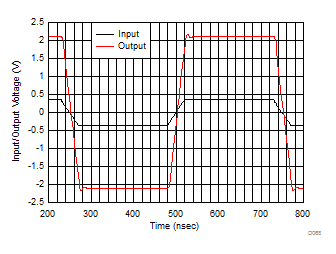
 Figure 7-9 Bipolar-Supply Step Response