ZHCSGM4D August   2017  – September 2024 OPA838

PRODMIX  

  1.   1
  2. 特性
  3. 应用
  4. 说明
  5. Device Comparison Table
  6. Pin Configuration and Functions
  7. Specifications
    1. 6.1 Absolute Maximum Ratings
    2. 6.2 ESD Ratings
    3. 6.3 Recommended Operating Conditions
    4. 6.4 Thermal Information
    5. 6.5 Electrical Characteristics VS = 5 V
    6. 6.6 Electrical Characteristics VS = 3 V
    7. 6.7 Typical Characteristics: VS = 5 V
    8. 6.8 Typical Characteristics: VS = 3 V
    9. 6.9 Typical Characteristics: Over Supply Range
  8. Detailed Description
    1. 7.1 Overview
    2. 7.2 Functional Block Diagram
    3. 7.3 Feature Description
      1. 7.3.1 Input Common-Mode Voltage Range
      2. 7.3.2 Output Voltage Range
      3. 7.3.3 Power-Down Operation
      4. 7.3.4 Trade-Offs in Selecting The Feedback Resistor Value
      5. 7.3.5 Driving Capacitive Loads
    4. 7.4 Device Functional Modes
      1. 7.4.1 Split-Supply Operation (±1.35 V to ±2.7 V)
      2. 7.4.2 Single-Supply Operation (2.7 V to 5.4 V)
      3. 7.4.3 Power Shutdown Operation
  9. Application and Implementation
    1. 8.1 Application Information
      1. 8.1.1 Noninverting Amplifier
      2. 8.1.2 Inverting Amplifier
      3. 8.1.3 Output DC Error Calculations
      4. 8.1.4 Output Noise Calculations
    2. 8.2 Typical Applications
      1. 8.2.1 High-Gain Differential I/O Designs
        1. 8.2.1.1 Design Requirements
        2. 8.2.1.2 Detailed Design Procedure
        3. 8.2.1.3 Application Curves
      2. 8.2.2 Transimpedance Amplifier
        1. 8.2.2.1 Design Requirements
        2. 8.2.2.2 Detailed Design Procedure
        3. 8.2.2.3 Application Curve
    3. 8.3 Power Supply Recommendations
    4. 8.4 Layout
      1. 8.4.1 Layout Guidelines
      2. 8.4.2 Layout Example
  10. Device and Documentation Support
    1. 9.1 Device Support
      1. 9.1.1 开发支持
        1. 9.1.1.1 TINA-TI™ 仿真软件(免费下载)
    2. 9.2 Documentation Support
      1. 9.2.1 Related Documentation
    3. 9.3 接收文档更新通知
    4. 9.4 支持资源
    5. 9.5 Trademarks
    6. 9.6 静电放电警告
    7. 9.7 术语表
  11. 10Revision History
  12. 11Mechanical, Packaging, and Orderable Information

封装选项

机械数据 (封装 | 引脚)
散热焊盘机械数据 (封装 | 引脚)
订购信息

Typical Characteristics: VS = 3 V

at VS+ = 3 V, VS– = 0 V, RF = 1 kΩ, RG = 200 Ω, RL = 2 kΩ, G = 6 V/V, input and output referenced to midsupply, and TA = 25°C (unless otherwise noted)
OPA838 Noninverting Small-Signal Response vs GainFigure 6-19 Noninverting Small-Signal Response vs Gain
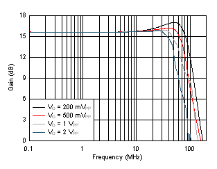
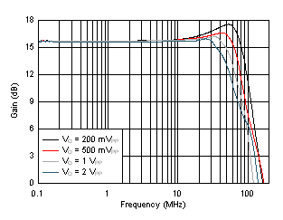
OPA838 Noninverting Large-Signal Bandwidth vs VOPP
See Figure 8-1 (AV = 6 V/V)
Figure 6-21 Noninverting Large-Signal Bandwidth vs VOPP
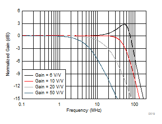
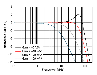
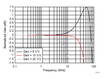
OPA838 Noninverting Response Flatness vs Gain
See Figure 8-1 and Table 8-1 (VO = 200 mVPP, R LOAD = 2 kΩ)
Figure 6-23 Noninverting Response Flatness vs Gain
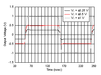
OPA838 Noninverting Step Response vs V OPPFigure 6-25 Noninverting Step Response vs V OPP
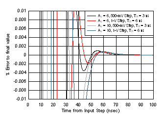
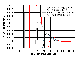
OPA838 Noninverting Settling TimeFigure 6-27 Noninverting Settling Time
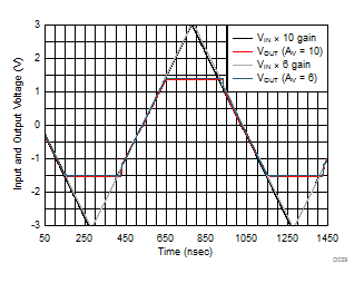
OPA838 Noninverting Overdrive RecoveryFigure 6-29 Noninverting Overdrive Recovery
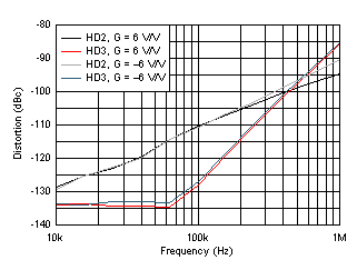
OPA838 Harmonic Distortion vs FrequencyFigure 6-31 Harmonic Distortion vs Frequency
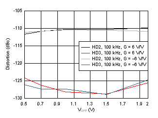
OPA838 Harmonic Distortion vs Output SwingFigure 6-33 Harmonic Distortion vs Output Swing
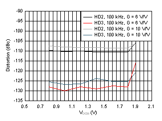
OPA838 Noninverting Harmonic Distortion vs Output Common-Mode Voltage
See Figure 8-1 and Table 8-1, VO = 1 VPP
Figure 6-35 Noninverting Harmonic Distortion vs Output Common-Mode Voltage
OPA838 Inverting Small-Signal Response vs GainFigure 6-20 Inverting Small-Signal Response vs Gain
OPA838 Inverting Large-Signal Bandwidth vs VOPP
See Figure 8-2 (AV = –6 V/V)
Figure 6-22 Inverting Large-Signal Bandwidth vs VOPP
OPA838 Inverting Response Flatness vs Gain
See Figure 8-2 and Table 8-2 (VO = 200 mVPP, R LOAD = 2 kΩ)
Figure 6-24 Inverting Response Flatness vs Gain
OPA838 Inverting Step Response vs VOPPFigure 6-26 Inverting Step Response vs VOPP
OPA838 Inverting Settling TimeFigure 6-28 Inverting Settling Time
OPA838 Inverting Overdrive RecoveryFigure 6-30 Inverting Overdrive Recovery
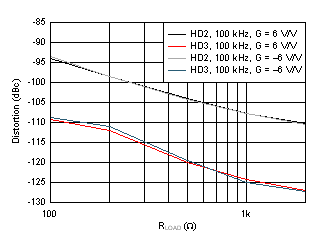
OPA838 Harmonic Distortion vs LoadFigure 6-32 Harmonic Distortion vs Load
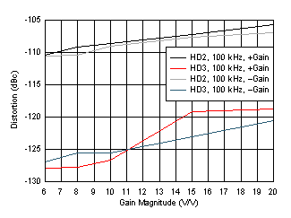
OPA838 Harmonic Distortion vs Gain
See Figure 8-1, Figure 8-2, Table 8-1, and Table 8-2
2-kΩ load, 2 VPP
Figure 6-34 Harmonic Distortion vs Gain
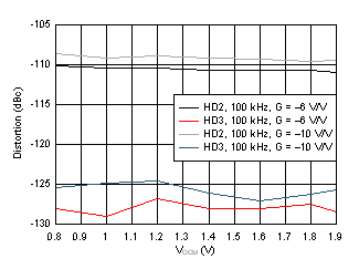
OPA838 Inverting Harmonic Distortion vs Output Common-Mode Voltage
See Figure 8-2 and Table 8-2, VO = 1 VPP
Figure 6-36 Inverting Harmonic Distortion vs Output Common-Mode Voltage