at VS+ = +2.5 V, VS– = –2.5 V, RF = 0 Ω, Gain = 1 V/V,
input common-mode biased at midsupply, RL = 200 Ω, output load referenced to
midsupply, and TA = 25°C (unless otherwise noted)
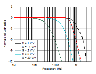
 Figure 7-1 Small-Signal
Response vs Gain
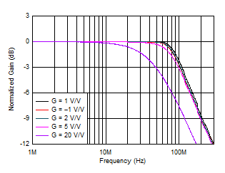
 Figure 7-3 Large-Signal
Response vs Gain
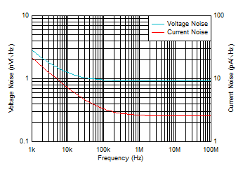
 Figure 7-5 Voltage and
Current Noise Density
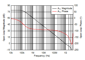
 Figure 7-7 Open-Loop Magnitude and
Phase
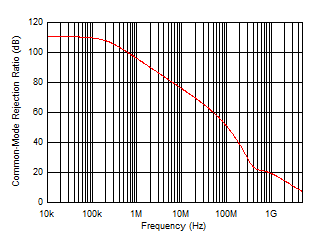
 Figure 7-9 Common-Mode Rejection Ratio
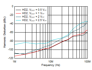
 Figure 7-11 Harmonic Distortion (HD2) vs
Output Swing
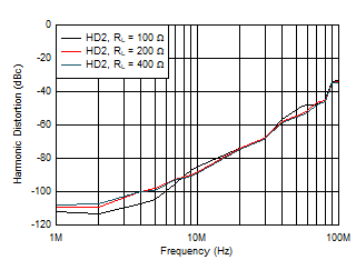
  Figure 7-13 Harmonic Distortion (HD2) vs Load
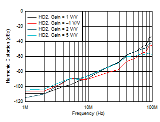
 Figure 7-15 Harmonic Distortion (HD2) vs Gain
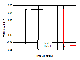
|
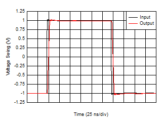
Average Rise and Fall Time (10% - 90%) = 680 ps |
|
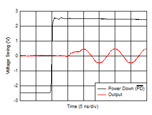
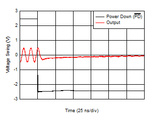
Figure 7-17 Small-Signal Transient Response Figure 7-19 Turnon Transient Response
|
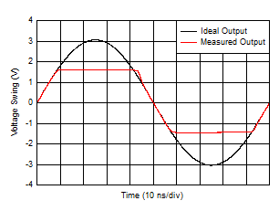
Gain = 5 V/V,
RF = 453 Ω, VIN = 1.25 VPP , 2x Output
Overdrive |
|
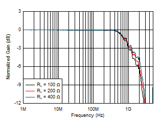
 Figure 7-2 Small-Signal
Response vs Output Load
| Gain = 20 V/V |
VOUT = 100 mVPP |
|
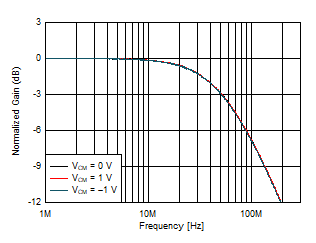
Figure 7-4 Gain Bandwidth
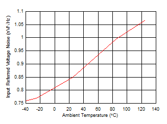
vs Common-Mode Figure 7-6 Voltage Noise
vs Temperature
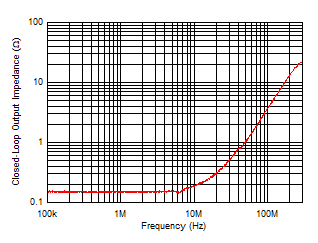
 Figure 7-8 Closed Loop Output
Impedance
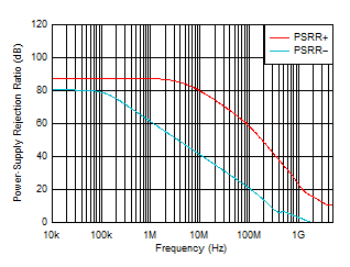
 Figure 7-10 Power Supply Rejection Ratio
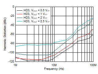
 Figure 7-12 Harmonic Distortion (HD3) vs
Output Swing
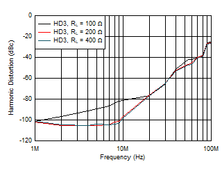
  Figure 7-14 Harmonic Distortion (HD3) vs Load
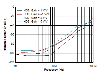
 Figure 7-16 Harmonic Distortion (HD3) vs Gain
|
Slew Rate: Rising = 365 V/µs, Falling = 346 V/µs |
|
 Figure 7-20 Turnoff
Transient Response