ZHCSBX2D December 2013 – August 2016 OPA857
PRODUCTION DATA.
7 Detailed Description
7.1 Overview
The OPA857 provides a unique combination of low-noise, high-bandwidth, and high-transimpedance gain. The amplifier is optimized to achieve greater than 100-MHz bandwidth on either the 5-kΩ or 20-kΩ transimpedance gain for the lowest possible RMS noise on the output for a targeted low input capacitance of
1.5 pF. Note that this 1.5-pF capacitance includes the board parasitic; thus, great attention must be placed on minimizing stray capacitance in the layout. This value is selected because the device is expected to be driven by a photodiode with biasing high enough to include the photodiode capacitance contribution between approximately 0.5 pF and 0.7 pF, leaving between 0.8 pF to 1 pF for the external parasitic.
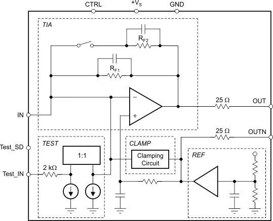
The OPA857 is a dedicated transimpedance amplifier with a pseudo-differential output. A block diagram is provided in the Functional Block Diagram section.
There are four distinct blocks in this diagram: a transimpedance amplifier (TIA), a reference voltage (REF), a test structure (TEST), and an internal clamping circuit (CLAMP).
The TIA block of the Functional Block Diagram includes two selectable gain configurations: RF1 and RF2. For a 500-Ω load, including the GND alternatives resulting from the internal 25-Ω series resistor on each output, the resulting gain is 4.5 kΩ or 18.2 kΩ. The TIA block is designed to provide excellent bandwidth (> 100 MHz) in both gain configurations with the lowest possible RMS noise over the entire bandwidth. This level of performance is achieved by minimizing the noise gain peaking at higher frequencies. The noise gain peaking resulting from feedback and source capacitance is the main noise contributor in high-speed transimpedance amplifiers.
The reference voltage block of the Functional Block Diagram has several purposes: this block provides an adequate dc reference voltage to the input, and provides a dc reference at the output (thus allowing the dc-coupled solution to interface to a fully-differential signal chain). The CMRR provided by the fully-differential signal chain reduces any feedthrough from the OPA857 power supply, thereby increasing the PSRR of the amplifier.
The test structure block is available on the pinout, but the main purpose of this structure is to allow the device characterization to proceed as smoothly as possible.
The internal clamping circuit block and ESD diodes on the IN pin are used for internal protection and to make sure that the amplifier can recover quickly after saturation.
These blocks are each described in further detail in the Feature Description section.
7.3 Feature Description
7.3.1 Transimpedance Amplifier (TIA) Block
The amplifier of the TIA block has a class-A output stage, which limits its usable swing from the common-mode voltage of 1.83 V to the negative rail. Because the internal protection allows excellent overdrive recovery, the negative swing cannot go closer than 0.6 V to the rail. The resulting output dynamic range of the OPA857 on a 3.3-V supply is 1.2 V. This 1.2-V swing corresponds to a maximum input current of 60 µA in the high-gain configuration, and 240 µA in the low-gain configuration. A 25-Ω series resistor between the internal output of the TIA block and OUT (pin 8) limits the amplifier load during short-circuit conditions. A similar 25-Ω series resistor also exists between the output of the reference voltage amplifier and OUTN (pin 5). The internal resistors on OUT and OUTN reduce the overall gain of the OPA857. With a 500-Ω differential load, the attenuation resulting from the load is 0.83 dB, which affects the overall transimpedance gain. Because of the load attenuation, the 20-kΩ transimpedance gain is reduced to an effective 18.2 kΩ, while the 5-kΩ internal resistor gain is reduced to an effective 4.5-kΩ internal resistor.
7.3.2 Reference Voltage (REF) Block
The reference output voltage is set to be 5/9th of the power supply. Thus, for a single 3.3-V supply, the reference voltage is 1.83 V. A wideband amplifier with low output impedance to high frequencies is used in the reference voltage block. The amplifier output drives two paths: the first path drives the output (OUTN) through a 25-Ω series resistor, while the second path drives the noninverting input of the TIA block. The output from the second path is filtered through an RC filter in order to reduce the noise contribution from the reference block.
7.3.3 Integrated Test Structure (TEST) Block
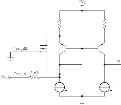
In order to evaluate the low input capacitance condition on the input of the OPA857, simply evaluate the OPA857 performance without the photodiode. An integrated voltage-to-current conversion is implemented and can be accessed with the use of Test_SD (pin 13) and Test_IN (pin 14). This V-to-I converter structure is represented in Figure 37. If required, a capacitor can be added to IN (pin 15) to match the target input capacitance during normal operation with an external photodiode. The test structure in Figure 37 allows for the evaluation of the OPA857 as a TIA using standard lab equipment, such as function generators and network analyzers.
 Figure 37. Internal V-to-I Converter
When using a photodiode, make sure that this source is turned off completely. This test structure is not intended to be used as a output dc-control voltage.
7.3.4 Internal Clamping Circuit (CLAMP) Block
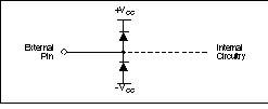
The OPA857 is built using a very high-speed, complementary, BICMOS process. The internal junction breakdown voltages are relatively low for these very small geometry devices. These breakdowns are reflected in the Absolute Maximum Ratings table. All device pins are protected with internal ESD protection diodes to the power supplies, as shown in Figure 38.
 Figure 38. Internal ESD Protection
These diodes provide moderate protection to input overdrive voltages above the supplies as well. The protection diodes can typically support 30-mA continuous current. Use additional external low-capacitance protection where higher currents are possible.
7.4 Device Functional Modes
7.4.1 Gain Control
The device transimpedance gain is controlled with the CTRL pin. Setting the CTRL pin high results in selecting the high-gain configuration. Setting the CTRL pin low results in selecting the low-gain configuration, as described in Table 1.
7.4.2 Test Mode
The OPA857 operates in normal mode when the input is driven by a photodiode. In test mode, the test structure described in the Integrated Test Structure (TEST) Block section is used to emulate a photodiode using a voltage input. Table 2 describes how to configure the OPA857 in each mode.
Table 2. Mode Configuration
| MODE | Test_IN PIN CONNECTED TO | Test_SD PIN CONNECTED TO |
|---|---|---|
| Normal mode | +VS | GND |
| Test mode | AC-coupled input using a series cap or dc-coupled signal on a 2.1-V (approx) offset voltage |
+VS |
Set an adequate dc voltage at the input to make sure that the output is operating within normal operation. At minimum, the output of the TIA block must be set to 5/9th of the supply voltage in preparation for a pulse configuration. For sine-wave operation, as required when measuring a frequency response, set the dc voltage on the OUT pin to allow the full sine-wave amplitude and avoid clipping. In such a case, the OUT pin voltage is set lower than 5/9th of the supply voltage.
Note that the 2-kΩ internal resistance used for the V-to-I conversion is not trimmed and can vary ±15% with process. Therefore, the source must be capable of sourcing both dc and ac voltages to make sure that the output voltage swing is compliant with the class-A output stage of the TIA block. Any change in the test circuit configuration (such as gain change) requires a new calibration of the internal V-to-I converter.
Again if a photodiode is used, the internal V-to-I converter must be shut off completely. Failure to do so results in degraded performance and higher than normal quiescent current.
