ZHCSMN4 February   2021 OPA858-Q1

PRODUCTION DATA  

  1. 特性
  2. 应用
  3. 说明
  4. Revision History
  5. Pin Configuration and Functions
  6. Specifications
    1. 6.1 Absolute Maximum Ratings
    2. 6.2 ESD Ratings
    3. 6.3 Recommended Operating Conditions
    4. 6.4 Thermal Information
    5. 6.5 Electrical Characteristics
    6. 6.6 Typical Characteristics
  7. Parameter Measurement Information
  8. Detailed Description
    1. 8.1 Overview
    2. 8.2 Functional Block Diagram
    3. 8.3 Feature Description
      1. 8.3.1 Input and ESD Protection
      2. 8.3.2 Feedback Pin
      3. 8.3.3 Wide Gain-Bandwidth Product
      4. 8.3.4 Slew Rate and Output Stage
      5. 8.3.5 Current Noise
    4. 8.4 Device Functional Modes
      1. 8.4.1 Split-Supply and Single-Supply Operation
      2. 8.4.2 Power-Down Mode
  9. Application and Implementation
    1. 9.1 Application Information
      1. 9.1.1 Using the OPA858-Q1 as a Transimpedance Amplifier
    2. 9.2 Typical Application
      1. 9.2.1 Design Requirements
      2. 9.2.2 Detailed Design Procedure
      3. 9.2.3 Application Curves
  10. 10Power Supply Recommendations
  11. 11Layout
    1. 11.1 Layout Guidelines
    2. 11.2 Layout Example
  12. 12Device and Documentation Support
    1. 12.1 Device Support
      1. 12.1.1 Development Support
    2. 12.2 Documentation Support
      1. 12.2.1 Related Documentation
    3. 12.3 Receiving Notification of Documentation Updates
    4. 12.4 支持资源
    5. 12.5 Trademarks
    6. 12.6 静电放电警告
    7. 12.7 术语表
  13. 13Mechanical, Packaging, and Orderable Information

封装选项

机械数据 (封装 | 引脚)
散热焊盘机械数据 (封装 | 引脚)
订购信息

Typical Characteristics

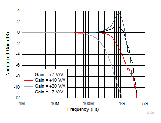
at VS+ = 2.5 V, VS– = –2.5 V, VIN+ = 0 V, RF = 453 Ω, Gain = 7 V/V, RL = 200 Ω, output load referenced to midsupply, and TA = 25°C (unless otherwise noted)
GUID-CCB324D6-67E5-4E7B-B6C2-2E2B9E80CFBB-low.gif
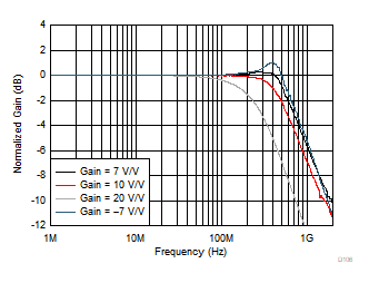
VOUT = 100 mVPP; see Figure 7-1 and Figure 7-2 for circuit configuration
Figure 6-1 Small-Signal Frequency Response vs Gain
GUID-60C1A3CC-7415-44CC-9D44-B7108DAF7FF2-low.gif
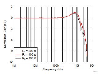
VOUT = 100 mVPP
Figure 6-3 Small-Signal Frequency Response vs Output Load
GUID-E2CF35DE-CD27-4AC1-906D-3EBBC66C85EB-low.gif
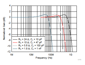
VOUT = 100 mVPP; see Figure 7-3 for circuit configuration
Figure 6-5 Small-Signal Frequency Response vs Capacitive Load
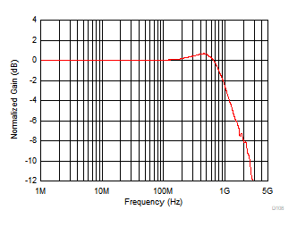
GUID-12252064-F582-4731-995B-821200514B3F-low.gif
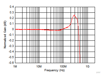
VOUT = 2 VPP
Figure 6-7 Large-Signal Response for 0.1-dB Gain Flatness
GUID-6AAA67CD-A9AD-4574-A6D0-E9D2E1D4F028-low.gif
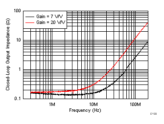
Small-Signal Response
Figure 6-9 Closed-Loop Output Impedance vs Frequency
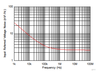
GUID-60612281-F9FA-4C3E-B130-1E4B974B72BD-low.gif
 
Figure 6-11 Voltage Noise Density vs Frequency
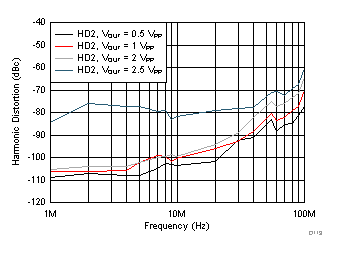
GUID-B250BAC7-0860-4D3F-BFD7-BBAD317E5ADD-low.gifFigure 6-13 Harmonic Distortion (HD2) vs Output Swing
GUID-0E53397A-009A-4F2B-8754-DA94D036AD1A-low.gif
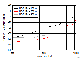
VOUT = 2 VPP
Figure 6-15 Harmonic Distortion (HD2) vs Output Load
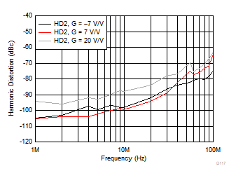
GUID-6A586801-1770-40B4-B38B-60A01D075D91-low.gif
VOUT = 2 VPP
Figure 6-17 Harmonic Distortion (HD2) vs Gain
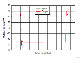
GUID-4E1C0C06-1D03-4107-9A67-DB6A5D435034-low.gif
Average Rise and Fall Time (10% - 90%) = 450 ps
Figure 6-19 Small-Signal Transient Response
GUID-ACA0A772-D815-4F17-A375-71FA204C3457-low.gif
 
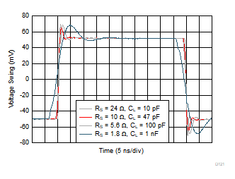
Figure 6-21 Small-Signal Transient Response vs Capacitive Load
GUID-05D2C240-23BE-4B2B-A04A-8991C577D10D-low.gif
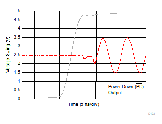
VS+ = 5 V, VS– = Ground
Figure 6-23 Turnon Transient Response
GUID-D985BFF0-7901-4926-B755-27DAAFD2C598-low.gif
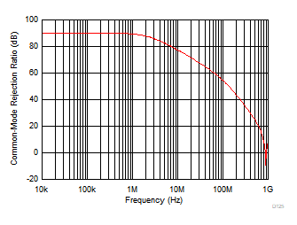
Small-Signal Response
Figure 6-25 Common-Mode Rejection Ratio vs Frequency
GUID-1DB418C8-8E58-4F82-ACB4-0218E99E98F2-low.gif
2 Typical Units
Figure 6-27 Quiescent Current vs Supply Voltage
GUID-4255C7CB-1C59-41D6-BE2C-BE2A16FC08A7-low.gif
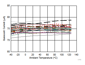
30 Units Tested
Figure 6-29 Quiescent Current (Amplifier Disabled) vs Ambient Temperature
GUID-F077187E-FF13-49BA-B965-980A916CC108-low.gif
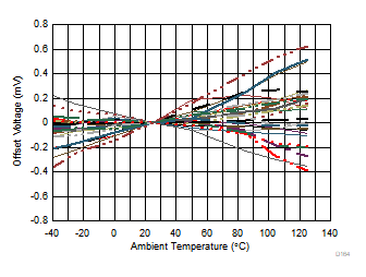
µ = 1 µV/°C σ = 2.2 µV/°C 28 Units Tested
Figure 6-31 Offset Voltage vs Ambient Temperature
GUID-C7E41E28-2D44-485F-AECF-A4F57A61115D-low.gif
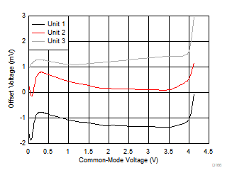
VS = 5 V 3 Typical Units
Figure 6-33 Offset Voltage vs Input Common-Mode Voltage
GUID-A7E01C14-E3DD-4EE1-A1A2-49EA75217BE6-low.gif
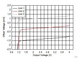
VS = 3.3 V 3 Typical Units
Figure 6-35 Offset Voltage vs Output Swing
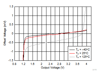
GUID-880362B3-6A9E-4E00-AF85-20C3DA446EF3-low.gif
 
Figure 6-37 Offset Voltage vs Output Swing vs Ambient Temperature
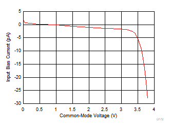
GUID-B110E818-EDFA-4F29-A177-04ACAC198744-low.gif
 
Figure 6-39 Input Bias Current vs Input Common-Mode Voltage
GUID-4D92156A-FB57-49A6-9E80-F5DC844EFC86-low.gif
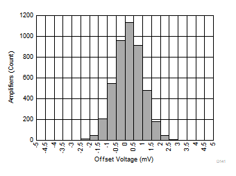
µ = –0.28 mV σ = 0.8 mV 4555 units tested
Figure 6-41 Offset Voltage Distribution
GUID-A260F7A7-9944-400E-B1AC-08B446C94B62-low.gif
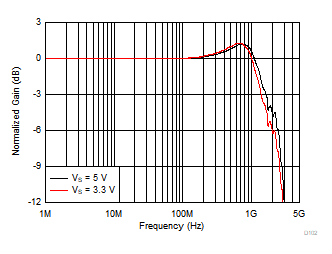
VOUT = 100 mVPP
Figure 6-2 Small-Signal Frequency Response vs Supply Voltage
GUID-BD744556-3AF7-4E1C-BEDE-5B658DBCDF56-low.gif
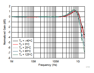
VOUT = 100 mVPP
Figure 6-4 Small-Signal Frequency Response vs Ambient Temperature
GUID-B70BF14E-A1B0-4B71-81C4-3C23FD25D233-low.gif
VOUT = 2 VPP
Figure 6-6 Large-Signal Frequency Response vs Gain
GUID-24288889-9D6C-482A-A5BA-A3F23694B6F7-low.gif
VS = 3.3 V VOUT = 1 VPP
Figure 6-8 Large-Signal Frequency Response
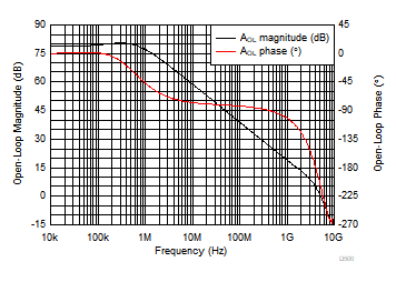
GUID-B206C3CE-2248-4812-BCD7-A375BE64FEBF-low.gif
Small-Signal Response
Figure 6-10 Open-Loop Magnitude and Phase vs Frequency
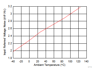
GUID-E3DBA7C5-D382-4ADB-9BC0-40AF6C94A1F8-low.gif
Frequency = 10 MHz
Figure 6-12 Voltage Noise Density vs Ambient Temperature
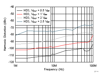
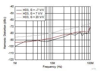
GUID-EB629C17-DB21-4252-A814-27B41CC6BA40-low.gifFigure 6-14 Harmonic Distortion (HD3) vs Output Swing
GUID-BE2649BF-A127-4E43-8D00-D43A76822995-low.gif
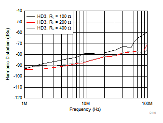
VOUT = 2 VPP
Figure 6-16 Harmonic Distortion (HD3) vs Output Load
GUID-D55A4693-3FA0-41EE-A459-B422CFE6EA89-low.gif
VOUT = 2 VPP
Figure 6-18 Harmonic Distortion (HD3) vs Gain
GUID-D3D87112-0B23-4603-9752-6ADC9CC56592-low.gif
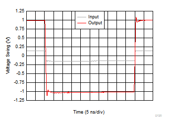
Average Rise and Fall Time (10% - 90%) = 750 ps
Figure 6-20 Large-Signal Transient Response
GUID-971B151E-AF79-4F69-8B2A-C40D63CB2AAD-low.gif
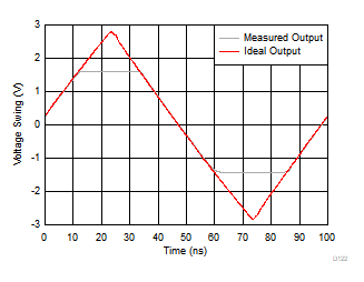
2x Output Overdrive
Figure 6-22 Output Overload Response
GUID-2CE8935F-2C5E-4D2F-8AAD-B41F26C70A11-low.gif
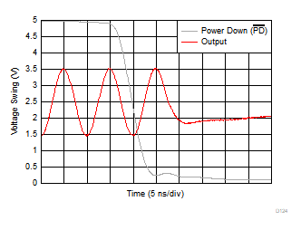
VS+ = 5 V, VS– = Ground
Figure 6-24 Turnoff Transient Response
GUID-9F424A41-36F5-4F2D-9BB1-B38099ABA765-low.gif
Small-Signal Response
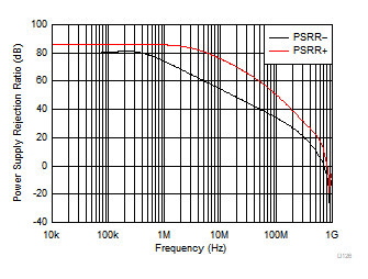
Figure 6-26 Power Supply Rejection Ratio vs Frequency
GUID-A30D2BB0-BBBB-4EC5-A66D-4CCEE9094E3E-low.gif
2 Typical Units
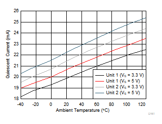
Figure 6-28 Quiescent Current vs Ambient Temperature
GUID-63E87532-ECCA-4925-B014-82E79D7BC4DA-low.gif
3 Typical Units
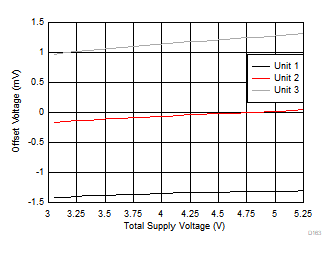
Figure 6-30 Offset Voltage vs Supply Voltage
GUID-887DDE81-4623-42A9-9E1C-5F206EE0AB77-low.gif
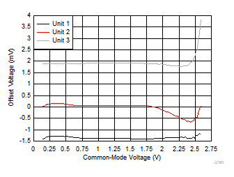
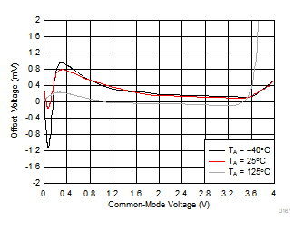
VS = 3.3 V 3 Typical Units
Figure 6-32 Offset Voltage vs Input Common-Mode Voltage
GUID-423677E7-7D7B-4D60-BD72-E5E985BF9A8E-low.gif
 
Figure 6-34 Offset Voltage vs Input Common-Mode Voltage vs Ambient Temperature
GUID-936A32B6-2AF4-41C4-9B1D-04D7C0C82FDB-low.gif
VS = 5 V 3 Typical Units
Figure 6-36 Offset Voltage vs Output Swing
GUID-7BF50F05-598C-4262-B0F2-BEBB34485BAC-low.gif
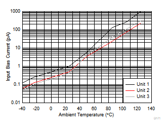
3 Typical Units
Figure 6-38 Input Bias Current vs Ambient Temperature
GUID-BECB3848-113B-488F-A9B5-E06C59A7DC9F-low.gif
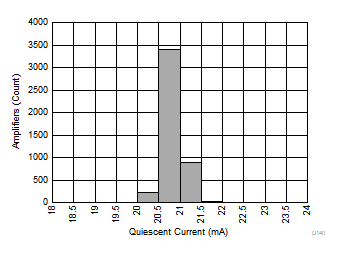
µ = 20.35 mA σ = 0.2 mA 4555 units tested
Figure 6-40 Quiescent Current Distribution
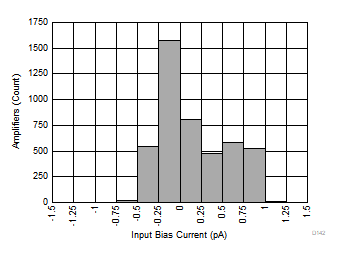
GUID-47E7F1F8-7044-4EC1-A603-3BD2D5332312-low.gif
µ = –0.1 pA σ = 0.39 pA 4555 units tested
Figure 6-42 Input Bias Current Distribution