ZHCSI18A April   2018  – July 2018 OPA858

PRODUCTION DATA.  

  1. 特性
  2. 应用
  3. 说明
    1.     Device Images
      1.      高速飞行时间接收器
      2.      光电二极管电容与带宽和噪声
  4. 修订历史记录
  5. Device Comparison Table
  6. Pin Configuration and Functions
    1.     Pin Functions
  7. Specifications
    1. 7.1 Absolute Maximum Ratings
    2. 7.2 ESD Ratings
    3. 7.3 Recommended Operating Conditions
    4. 7.4 Thermal Information
    5. 7.5 Electrical Characteristics
    6. 7.6 Typical Characteristics
  8. Parameter Measurement Information
    1. 8.1 Parameter Measurement Information
  9. Detailed Description
    1. 9.1 Overview
    2. 9.2 Functional Block Diagram
    3. 9.3 Feature Description
      1. 9.3.1 Input and ESD Protection
      2. 9.3.2 Feedback Pin
      3. 9.3.3 Wide Gain-Bandwidth Product
      4. 9.3.4 Slew Rate and Output Stage
      5. 9.3.5 Current Noise
    4. 9.4 Device Functional Modes
      1. 9.4.1 Split-Supply and Single-Supply Operation
      2. 9.4.2 Power-Down Mode
  10. 10Application and Implementation
    1. 10.1 Application Information
      1. 10.1.1 Using the OPA858 as a Transimpedance Amplifier
    2. 10.2 Typical Application
      1. 10.2.1 Design Requirements
      2. 10.2.2 Detailed Design Procedure
      3. 10.2.3 Application Curves
  11. 11Power Supply Recommendations
  12. 12Layout
    1. 12.1 Layout Guidelines
    2. 12.2 Layout Example
  13. 13器件和文档支持
    1. 13.1 接收文档更新通知
    2. 13.2 社区资源
    3. 13.3 商标
    4. 13.4 静电放电警告
    5. 13.5 术语表
  14. 14机械、封装和可订购信息

封装选项

机械数据 (封装 | 引脚)
散热焊盘机械数据 (封装 | 引脚)
订购信息

Current Noise

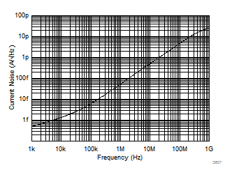
The input impedance of CMOS and JFET input amplifiers at low frequencies exceed several GΩs. However, at higher frequencies, the transistors parasitic capacitance to the drain, source, and substrate reduces the impedance. The high impedance at low frequencies eliminates any bias current and the associated shot noise. At higher frequencies, the input current noise increases (see Figure 53) as a result of capacitive coupling between the CMOS gate oxide and the underlying transistor channel. This phenomenon is a natural artifact of the construction of the transistor and is unavoidable.
OPA858 D607_SBOS852.gifFigure 53. Input Current Noise (IBN and IBI) vs Frequency