ZHCSMN5 February   2021 OPA859-Q1

PRODUCTION DATA  

  1. 特性
  2. 应用
  3. 说明
  4. Revision History
  5. Pin Configuration and Functions
  6. Specifications
    1. 6.1 Absolute Maximum Ratings
    2. 6.2 ESD Ratings
    3. 6.3 Recommended Operating Conditions
    4. 6.4 Thermal Information
    5. 6.5 Electrical Characteristics
    6. 6.6 Typical Characteristics
  7. Parameter Measurement Information
  8. Detailed Description
    1. 8.1 Overview
    2. 8.2 Functional Block Diagram
    3. 8.3 Feature Description
      1. 8.3.1 Input and ESD Protection
      2. 8.3.2 Feedback Pin
      3. 8.3.3 Wide Gain-Bandwidth Product
      4. 8.3.4 Slew Rate and Output Stage
      5. 8.3.5 Current Noise
    4. 8.4 Device Functional Modes
      1. 8.4.1 Split-Supply and Single-Supply Operation
      2. 8.4.2 Power-Down Mode
  9. Application and Implementation
    1. 9.1 Application Information
    2. 9.2 Typical Application
      1. 9.2.1 Design Requirements
      2. 9.2.2 Detailed Design Procedure
      3. 9.2.3 Application Curves
  10. 10Power Supply Recommendations
  11. 11Layout
    1. 11.1 Layout Guidelines
    2. 11.2 Layout Example
  12. 12Device and Documentation Support
    1. 12.1 Device Support
      1. 12.1.1 Development Support
    2. 12.2 Documentation Support
      1. 12.2.1 Related Documentation
    3. 12.3 Receiving Notification of Documentation Updates
    4. 12.4 支持资源
    5. 12.5 Trademarks
    6. 12.6 静电放电警告
    7. 12.7 术语表
  13. 13Mechanical, Packaging, and Orderable Information

封装选项

机械数据 (封装 | 引脚)
散热焊盘机械数据 (封装 | 引脚)
订购信息

Input and ESD Protection

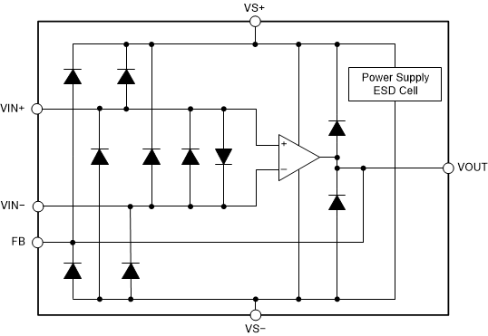
The OPA859-Q1 is fabricated on a low-voltage, high-speed, BiCMOS process. The internal, junction breakdown voltages are low for these small geometry devices, and as a result, all device pins are protected with internal ESD protection diodes to the power supplies as Figure 8-3 shows. There are two antiparallel diodes between the inputs of the amplifier that clamp the inputs during an overrange or fault condition.
GUID-9B9B0A8D-B619-430C-A5DF-B720765BEA87-low.gifFigure 8-3 Internal ESD Structure