ZHCSIQ9 September   2018 OPA859

PRODUCTION DATA.  

  1. 特性
  2. 应用
  3. 说明
    1.     Device Images
      1.      高速飞行时间接收器
      2.      光电二极管电容与带宽和噪声间的关系
  4. 修订历史记录
  5. Device Comparison Table
  6. Pin Configuration and Functions
    1.     Pin Functions
  7. Specifications
    1. 7.1 Absolute Maximum Ratings
    2. 7.2 ESD Ratings
    3. 7.3 Recommended Operating Conditions
    4. 7.4 Thermal Information
    5. 7.5 Electrical Characteristics
    6. 7.6 Typical Characteristics
  8. Parameter Measurement Information
    1. 8.1 Parameter Measurement Information
  9. Detailed Description
    1. 9.1 Overview
    2. 9.2 Functional Block Diagram
    3. 9.3 Feature Description
      1. 9.3.1 Input and ESD Protection
      2. 9.3.2 Feedback Pin
      3. 9.3.3 Wide Gain-Bandwidth Product
      4. 9.3.4 Slew Rate and Output Stage
      5. 9.3.5 Current Noise
    4. 9.4 Device Functional Modes
      1. 9.4.1 Split-Supply and Single-Supply Operation
      2. 9.4.2 Power-Down Mode
  10. 10Application and Implementation
    1. 10.1 Application Information
    2. 10.2 Typical Application
      1. 10.2.1 Design Requirements
      2. 10.2.2 Detailed Design Procedure
      3. 10.2.3 Application Curves
  11. 11Power Supply Recommendations
  12. 12Layout
    1. 12.1 Layout Guidelines
    2. 12.2 Layout Example
  13. 13器件和文档支持
    1. 13.1 器件支持
      1. 13.1.1 开发支持
    2. 13.2 文档支持
      1. 13.2.1 相关文档
    3. 13.3 接收文档更新通知
    4. 13.4 社区资源
    5. 13.5 商标
    6. 13.6 静电放电警告
    7. 13.7 术语表
  14. 14机械、封装和可订购信息

封装选项

机械数据 (封装 | 引脚)
散热焊盘机械数据 (封装 | 引脚)
订购信息

Typical Characteristics

at TA = 25°C, VS+ = 2.5 V, VS– = –2.5 V, VIN+ = 0 V, Gain = 1 V/V, RF = 0 Ω, RL = 200 Ω, and output load referenced to midsupply (unless otherwise noted)
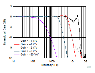
OPA859 D300_SBOS852.gif
VOUT = 100 mVPP; see Parameter Measurement Information for circuit configuration
Figure 1. Small-Signal Frequency Response vs Gain
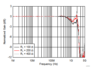
OPA859 D303_SBOS852.gif
VOUT = 100 mVPP
Figure 3. Small-Signal Frequency Response vs Output Load
OPA859 D301_SBOS852.gif
Gain = 20 V/V RF = 453 Ω
Figure 5. Frequency Response at Gain = 20 V/V
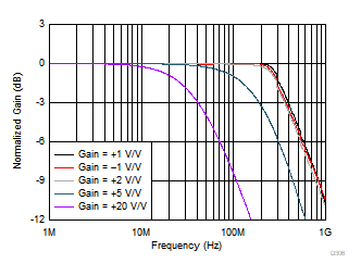
OPA859 D306_SBOS852.gif
VOUT = 2 VPP
Figure 7. Large-Signal Frequency Response vs Gain
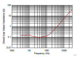
OPA859 D309_SBOS852.gif
Small-Signal Response
Figure 9. Closed-Loop Output Impedance vs Frequency
OPA859 D311_SBOS852.gif
Figure 11. Voltage Noise Density vs Frequency
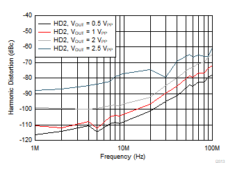
OPA859 D313_SBOS852.gif
Figure 13. Harmonic Distortion (HD2) vs Output Swing
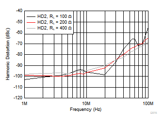
OPA859 D315_SBOS852.gif
VOUT = 2 VPP
Figure 15. Harmonic Distortion (HD2) vs Output Load
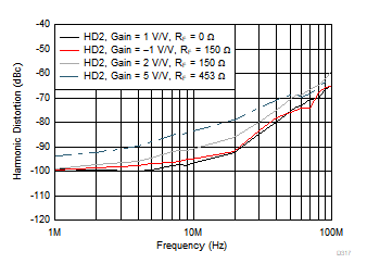
OPA859 D317_SBOS852.gif
VOUT = 2 VPP
Figure 17. Harmonic Distortion (HD2) vs Gain
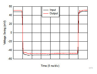
OPA859 D319_SBOS852.gif
Average Rise and Fall Time (10% - 90%) = 450 ps
Figure 19. Small-Signal Transient Response
OPA859 D321_SBOS852.gif
See Figure 46 for circuit configuration
Figure 21. Small-Signal Transient Response vs Capacitive Load
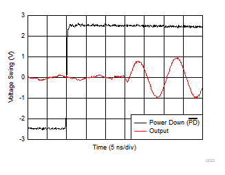
OPA859 D323_SBOS852.gif
Figure 23. Turnon Transient Response
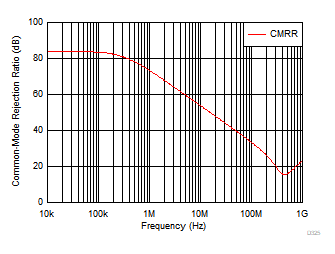
OPA859 D325_SBOS852.gif
Small-Signal Response
Figure 25. Common-Mode Rejection Ratio vs Frequency
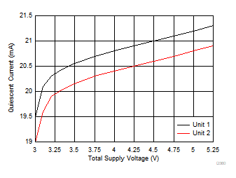
OPA859 D360_SBOS852.gif
2 Typical Units
Figure 27. Quiescent Current vs Supply Voltage
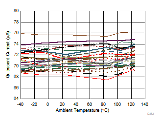
OPA859 D362_SBOS852.gif
32 Units Tested
Figure 29. Quiescent Current (Amplifier Disabled) vs Ambient Temperature
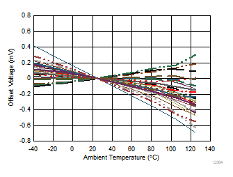
OPA859 D364_SBOS852.gif
µ = –2.1 µV/°C σ = 2 µV/°C 32 Units Tested
Figure 31. Offset Voltage vs Ambient Temperature
OPA859 D367_SBOS852.gif
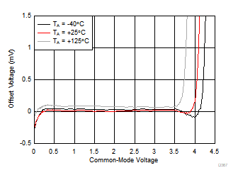
VS = 5 V
Figure 33. Offset Voltage vs Input Common-Mode Voltage vs Ambient Temperature
OPA859 D370_SBOS852.gif
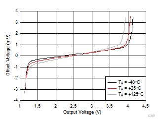
VS = 5 V
Figure 35. Offset Voltage vs Output Swing vs Ambient Temperature
OPA859 D372_SBOS852.gif
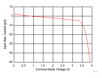
VS = 5 V
Figure 37. Input Bias Current vs Input Common-Mode Voltage
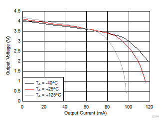
OPA859 D374_SBOS852.gif
VS = 5 V
Figure 39. Output Swing vs Sourcing Current
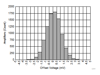
OPA859 D341_SBOS852.gif
µ = –0.38 mV σ = 0.97 mV 9150 Units Tested
Figure 41. Offset Voltage Distribution
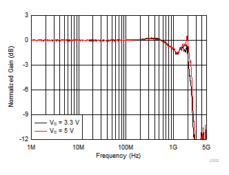
OPA859 D302_SBOS852.gif
VOUT = 100 mVPP
Figure 2. Small-Signal Frequency Response vs Supply Voltage
OPA859 D304_SBOS852.gif
VOUT = 100 mVPP
Figure 4. Small-Signal Frequency Response vs Ambient Temperature
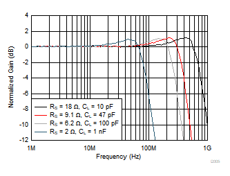
OPA859 D305_SBOS852.gif
VOUT = 100 mVPP, See Figure 46 for circuit configuration
Figure 6. Small-Signal Frequency Response vs Capacitive Load
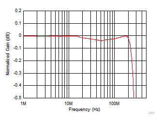
OPA859 D307_SBOS852.gif
VOUT = 2 VPP
Figure 8. Large-Signal Response for 0.1-dB Gain Flatness
OPA859 D310_SBOS852.gif
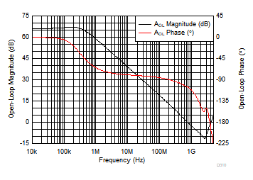
Small-Signal Response
Figure 10. Open-Loop Magnitude and Phase vs Frequency
OPA859 D312_SBOS852.gif
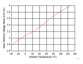
Frequency 10 MHz
Figure 12. Voltage Noise Density vs Ambient Temperature
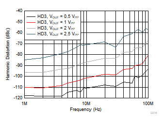
OPA859 D314_SBOS852.gif
Figure 14. Harmonic Distortion (HD3) vs Output Swing
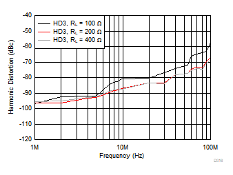
OPA859 D316_SBOS852.gif
VOUT = 2 VPP
Figure 16. Harmonic Distortion (HD3) vs Output Load
OPA859 D318_SBOS852.gif
VOUT = 2 VPP
Figure 18. Harmonic Distortion (HD3) vs Gain
OPA859 D320_SBOS852.gif
Slew Rate: Falling = 1160 V/µs, Rising = 1400 V/µs
Figure 20. Large-Signal Transient Response
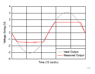
OPA859 D322_SBOS852.gif
Gain = 5 V/V, RF = 453 Ω, 2x Output Overdrive
Figure 22. Output Overload Response
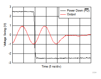
OPA859 D324_SBOS852.gif
Figure 24. Turnoff Transient Response
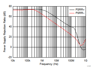
OPA859 D326_SBOS852.gif
Small-Signal Response
Figure 26. Power Supply Rejection Ratio vs Frequency
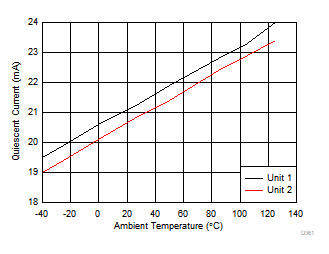
OPA859 D361_SBOS852.gif
VS = 5 V 2 Typical Units
Figure 28. Quiescent Current vs Ambient Temperature
OPA859 D363_SBOS852.gif
3 Typical Units
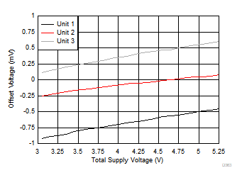
Figure 30. Offset Voltage vs Supply Voltage
OPA859 D366_SBOS852.gif
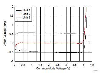
VS = 5 V 3 Typical Units
Figure 32. Offset Voltage vs Input Common-Mode Voltage
OPA859 D369_SBOS852.gif
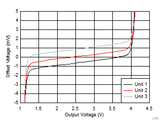
VS = 5 V 3 Typical Units
Figure 34. Offset Voltage vs Output Swing
OPA859 D371_SBOS852.gif
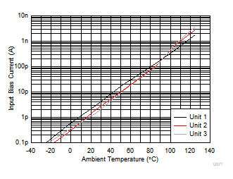
3 Typical Units
Figure 36. Input Bias Current vs Ambient Temperature
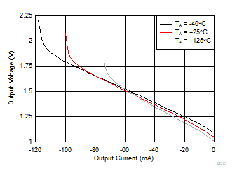
OPA859 D373_SBOS852.gif
VS = 5 V
Figure 38. Output Swing vs Sinking Current
OPA859 D340_SBOS852.gif
µ = 20.8 mA σ = 0.25 mA 9150 Units Tested
Figure 40. Quiescent Current Distribution
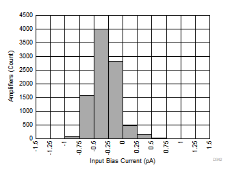
OPA859 D342_SBOS852.gif
µ = –0.55 pA σ = 0.23 pA 9150 Units Tested
Figure 42. Input Bias Current Distribution