ZHCSIQ9 September   2018 OPA859

PRODUCTION DATA.  

  1. 特性
  2. 应用
  3. 说明
    1.     Device Images
      1.      高速飞行时间接收器
      2.      光电二极管电容与带宽和噪声间的关系
  4. 修订历史记录
  5. Device Comparison Table
  6. Pin Configuration and Functions
    1.     Pin Functions
  7. Specifications
    1. 7.1 Absolute Maximum Ratings
    2. 7.2 ESD Ratings
    3. 7.3 Recommended Operating Conditions
    4. 7.4 Thermal Information
    5. 7.5 Electrical Characteristics
    6. 7.6 Typical Characteristics
  8. Parameter Measurement Information
    1. 8.1 Parameter Measurement Information
  9. Detailed Description
    1. 9.1 Overview
    2. 9.2 Functional Block Diagram
    3. 9.3 Feature Description
      1. 9.3.1 Input and ESD Protection
      2. 9.3.2 Feedback Pin
      3. 9.3.3 Wide Gain-Bandwidth Product
      4. 9.3.4 Slew Rate and Output Stage
      5. 9.3.5 Current Noise
    4. 9.4 Device Functional Modes
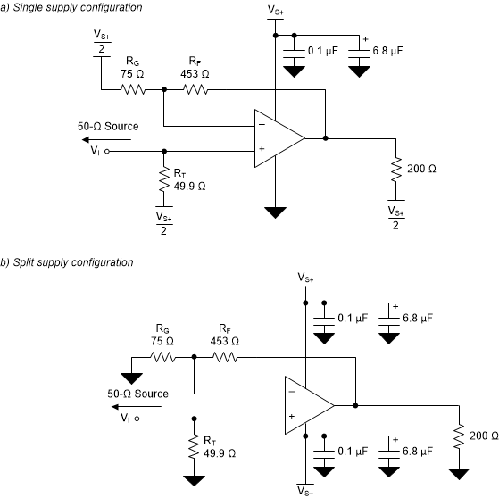
      1. 9.4.1 Split-Supply and Single-Supply Operation
      2. 9.4.2 Power-Down Mode
  10. 10Application and Implementation
    1. 10.1 Application Information
    2. 10.2 Typical Application
      1. 10.2.1 Design Requirements
      2. 10.2.2 Detailed Design Procedure
      3. 10.2.3 Application Curves
  11. 11Power Supply Recommendations
  12. 12Layout
    1. 12.1 Layout Guidelines
    2. 12.2 Layout Example
  13. 13器件和文档支持
    1. 13.1 器件支持
      1. 13.1.1 开发支持
    2. 13.2 文档支持
      1. 13.2.1 相关文档
    3. 13.3 接收文档更新通知
    4. 13.4 社区资源
    5. 13.5 商标
    6. 13.6 静电放电警告
    7. 13.7 术语表
  14. 14机械、封装和可订购信息

封装选项

机械数据 (封装 | 引脚)
散热焊盘机械数据 (封装 | 引脚)
订购信息

Power Supply Recommendations

The OPA859 operates on supplies from 3.3 V to 5.25 V. The OPA859 operates on single-sided supplies, split and balanced bipolar supplies, and unbalanced bipolar supplies. Because the OPA859 does not feature rail-to-rail inputs or outputs, the input common-mode and output swing ranges are limited at 3.3-V supplies.
OPA859 OPA85x_supply_config_sbos852.gifFigure 60. Split and Single Supply Circuit Configuration , Gain = 7 V/V