ZHCSK39C August 2019 – August 2020 OPA862
PRODUCTION DATA
- 1 特性
- 2 应用
- 3 说明
- 4 Revision History
- 5 Pin Configuration and Functions
-
6 Specifications
- 6.1 Absolute Maximum Ratings
- 6.2 ESD Ratings
- 6.3 Recommended Operating Conditions
- 6.4 Thermal Information
- 6.5 Electrical Characteristics: VS = ±2.5 V to ±5 V
- 6.6 Typical Characteristics: VS = ±5 V
- 6.7 Typical Characteristics: VS = ±2.5 V
- 6.8 Typical Characteristics: VS = 1.9 V, –1.4 V
- 6.9 Typical Characteristics: VS = 1.9 V, –1.4 V to ±5 V
- 7 Detailed Description
- 8 Application and Implementation
- 9 Power Supply Recommendations
- 10Layout
- 11Device and Documentation Support
- 12Mechanical, Packaging, and Orderable Information
8.2.3 DC Level-Shifting
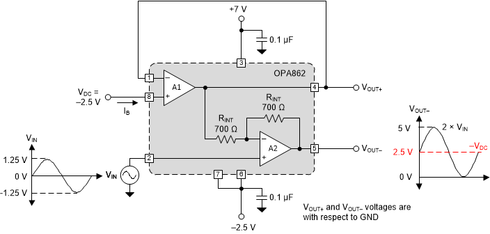
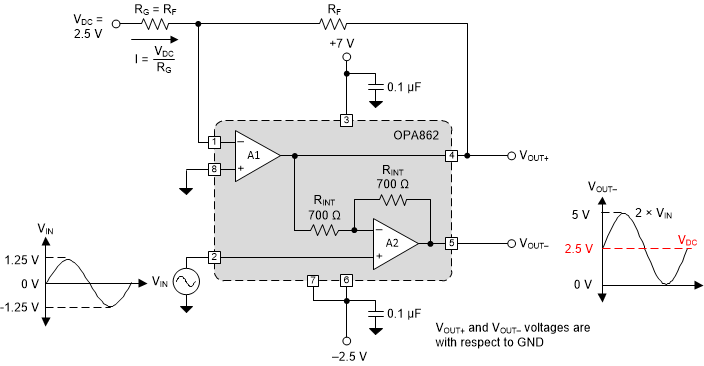
Often, applications must level-shift a ground-referenced signal to a non-ground voltage. Configurations in Figure 8-10 and Figure 8-11 show two different ways of level-shifting a signal by using the OPA862 without having to use external resistors, saving board cost and space. These configurations leverage the fixed noninverting gain-of-2 configuration of A2 and the summing configuration of A1 to level-shift the signal at VOUT–. The internal resistors of the OPA862 are extremely well-matched to maintain the gain-of-2 accuracy of A2. Similarly matched external resistors can add significant cost to the system and often are more expensive than the amplifier itself.
Apart from the polarity of the VDC-shift at the output, a key difference between the configurations of Figure 8-10 and Figure 8-11 is that in the case of Figure 8-10, VDC only must be capable of driving the IB of A1 but in the case of Figure 8-11, VDC must be capable of driving higher currents, as given by I = VDC / RG when a noninverting input of A1 is grounded.
 Figure 8-10 Level-Shifting With a DC Source of Polarity Opposite to the Desired DC Shift
 Figure 8-11 Level-Shifting With a DC Source of Polarity Same as the Desired DC Shift