ZHCSK39C August 2019 – August 2020 OPA862
PRODUCTION DATA
- 1 特性
- 2 应用
- 3 说明
- 4 Revision History
- 5 Pin Configuration and Functions
-
6 Specifications
- 6.1 Absolute Maximum Ratings
- 6.2 ESD Ratings
- 6.3 Recommended Operating Conditions
- 6.4 Thermal Information
- 6.5 Electrical Characteristics: VS = ±2.5 V to ±5 V
- 6.6 Typical Characteristics: VS = ±5 V
- 6.7 Typical Characteristics: VS = ±2.5 V
- 6.8 Typical Characteristics: VS = 1.9 V, –1.4 V
- 6.9 Typical Characteristics: VS = 1.9 V, –1.4 V to ±5 V
- 7 Detailed Description
- 8 Application and Implementation
- 9 Power Supply Recommendations
- 10Layout
- 11Device and Documentation Support
- 12Mechanical, Packaging, and Orderable Information
8.2.2 Transimpedance Amplifier Configuration
With recent advancements in light-sensing technology, transimpedance (TIA) applications are becoming popular, ranging in signal bandwidth needs from tens of kHz to hundreds of MHz. Because the current output of the photodiode in these TIA applications is unipolar, a key challenge in interfacing with the fully differential input analog-to-digital converters (ADCs) is maximizing the differential signal to the ADC in order to maximize the signal-to-noise ratio (SNR).
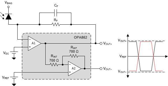
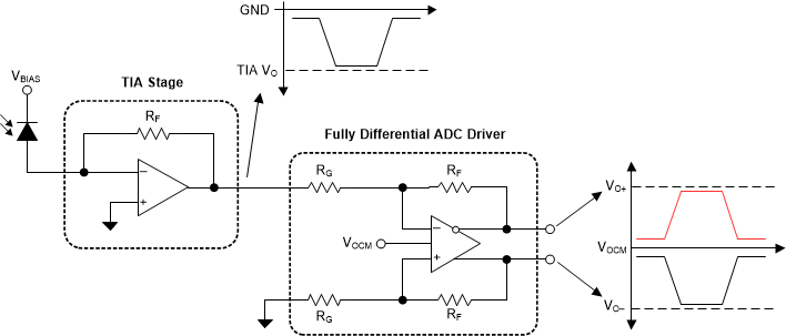
As illustrated in the output waveform of Figure 8-6, only half the differential output signal swing of the FDA is available. On the contrary, by using the OPA862 as the TIA stage, a single-device interface to the ADC can be designed that also allows the full differential swing to the ADC and set the desired output common-mode as shown in Figure 8-5. VREF is used to set the output common-mode voltage and VDC is used to DC shift the outputs such that for a zero photodiode current, VOD (equal to VOUT+ – VOUT–) is at one of the peaks of the desired differential peak-to-peak swing. Whether the VOD peak at the zero photodiode current is at a high or low peak is determined by the direction of current through RF in the presence of the photodiode signal current.
 Figure 8-5 Improved TIA Signal Chain With the OPA862
 Figure 8-6 Conventional TIA Signal Chain