ZHCSMO3J june 2020 – june 2023 OPA2863 , OPA4863 , OPA863
PRODUCTION DATA
- 1
- 1 特性
- 2 应用
- 3 说明
- 4 Revision History
- 5 Device Comparison Table
- 6 Pin Configuration and Functions
-
7 Specifications
- 7.1 Absolute Maximum Ratings
- 7.2 ESD Ratings
- 7.3 Recommended Operating Conditions
- 7.4 Thermal Information: OPA863
- 7.5 Thermal Information: OPA2863
- 7.6 Thermal Information: OPA4863
- 7.7 Electrical Characteristics: VS = 10 V
- 7.8 Electrical Characteristics: VS = 3 V
- 7.9 Typical Characteristics: VS = 10 V
- 7.10 Typical Characteristics: VS = 3 V
- 7.11 Typical Characteristics: VS = 3 V to 10 V
- 8 Detailed Description
- 9 Application and Implementation
- 10Device and Documentation Support
- 11Mechanical, Packaging, and Orderable Information
6 Pin Configuration and Functions
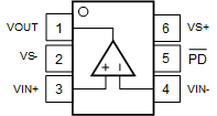
 Figure 6-1 OPA863 DBV Package,
6-Pin SOT-23
(Top View)
 Figure 6-2 OPA863 DBV Package,
5-Pin SOT-23
(Top View)
Table 6-1 Pin Functions: OPA863
| PIN | TYPE(1) | DESCRIPTION | ||
|---|---|---|---|---|
| NAME | NO. | |||
| DBV (SOT-23, 5) | DBV (SOT-23, 6) | |||
| PD | — | 5 | I | Power down. Low = disabled, high = normal operation (pin must be driven). |
| VIN+ | 3 | 3 | I | Noninverting input pin |
| VIN– | 4 | 4 | I | Inverting input pin |
| VOUT | 1 | 1 | O | Output pin |
| VS– | 2 | 2 | P | Negative power-supply pin |
| VS+ | 5 | 6 | P | Positive power-supply pin |
(1) I = input, O = output, and P = power.
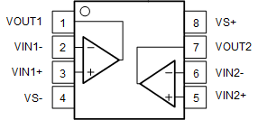
 Figure 6-3 OPA2863 D Package, 8-Pin
SOIC
Figure 6-3 OPA2863 D Package, 8-Pin
SOICand DGK Package, 8-Pin VSSOP,
(Top View)
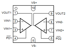
 Figure 6-4 OPA2863 RUN Package,
10-Pin WQFN
(Top View)
Table 6-2 Pin Functions: OPA2863
| PIN | TYPE(1) | DESCRIPTION | ||
|---|---|---|---|---|
| NAME | NO. | |||
| D (SOIC), DGK (VSSOP) | RUN (WQFN) | |||
| PD1 | — | 4 | I | Amplifier 1 power down. Low = disabled, high = normal operation (pin must be driven). |
| PD2 | — | 6 | I | Amplifier 2 power down. Low = disabled, high = normal operation (pin must be driven). |
| VIN1– | 2 | 2 | I | Amplifier 1 inverting input pin |
| VIN1+ | 3 | 3 | I | Amplifier 1 noninverting input pin |
| VIN2– | 6 | 8 | I | Amplifier 2 inverting input pin |
| VIN2+ | 5 | 7 | I | Amplifier 2 noninverting input pin |
| VOUT1 | 1 | 1 | O | Amplifier 1 output pin |
| VOUT2 | 7 | 9 | O | Amplifier 2 output pin |
| VS– | 4 | 5 | P | Negative power-supply pin |
| VS+ | 8 | 10 | P | Positive power-supply pin |
(1) I = input, O = output, and P = power.
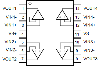
 Figure 6-5 OPA4863 PW Package,
14-Pin TSSOP
(Top View)
Table 6-3 Pin Functions: OPA4863
| PIN | TYPE(1) | DESCRIPTION | |
|---|---|---|---|
| NAME | NO. | ||
| VIN1– | 2 | I | Amplifier 1 inverting input pin |
| VIN1+ | 3 | I | Amplifier 1 noninverting input pin |
| VIN2– | 6 | I | Amplifier 2 inverting input pin |
| VIN2+ | 5 | I | Amplifier 2 noninverting input pin |
| VIN3– | 9 | I | Amplifier 3 inverting input pin |
| VIN3+ | 10 | I | Amplifier 3 noninverting input pin |
| VIN4– | 13 | I | Amplifier 4 inverting input pin |
| VIN4+ | 12 | I | Amplifier 4 noninverting input pin |
| VOUT1 | 1 | O | Amplifier 1 output pin |
| VOUT2 | 7 | O | Amplifier 2 output pin |
| VOUT3 | 8 | O | Amplifier 3 output pin |
| VOUT4 | 14 | O | Amplifier 4 output pin |
| VS– | 11 | P | Negative power-supply pin |
| VS+ | 4 | P | Positive power-supply pin |
(1) I = input, O = output, and P = power.