ZHCSOS5F May   2022  – October 2024 OPA2863A , OPA863A

PRODMIX  

  1.   1
  2. 特性
  3. 应用
  4. 说明
  5. Device Comparison Table
  6. Pin Configuration and Functions
  7. Specifications
    1. 6.1  Absolute Maximum Ratings
    2. 6.2  ESD Ratings
    3. 6.3  Recommended Operating Conditions
    4. 6.4  Thermal Information OPA863A
    5. 6.5  Thermal Information OPA2863A
    6. 6.6  Electrical Characteristics VS = ±5 V
    7. 6.7  Electrical Characteristics VS = 3 V
    8. 6.8  Typical Characteristics: VS = ±5 V
    9. 6.9  Typical Characteristics: VS = 3 V
    10. 6.10 Typical Characteristics: VS = 3 V to 10 V
  8. Detailed Description
    1. 7.1 Overview
    2. 7.2 Functional Block Diagram
    3. 7.3 Feature Description
      1. 7.3.1 Input Stage
      2. 7.3.2 Output Stage
        1. 7.3.2.1 Overload Power Limit
      3. 7.3.3 ESD Protection
    4. 7.4 Device Functional Modes
      1. 7.4.1 Power-Down Mode
  9. Application and Implementation
    1. 8.1 Application Information
    2. 8.2 Typical Applications
      1. 8.2.1 Active Filters
        1. 8.2.1.1 Design Requirements
        2. 8.2.1.2 Detailed Design Procedure
        3. 8.2.1.3 Application Curves
      2. 8.2.2 Low-Power SAR ADC Driver and Reference Buffer
    3. 8.3 Power Supply Recommendations
    4. 8.4 Layout
      1. 8.4.1 Layout Guidelines
      2. 8.4.2 Layout Example
  10. Device and Documentation Support
    1. 9.1 Documentation Support
      1. 9.1.1 Related Documentation
    2. 9.2 接收文档更新通知
    3. 9.3 支持资源
    4. 9.4 Trademarks
    5. 9.5 静电放电警告
    6. 9.6 术语表
  11. 10Revision History
  12. 11Mechanical, Packaging, and Orderable Information

封装选项

请参考 PDF 数据表获取器件具体的封装图。

机械数据 (封装 | 引脚)
  • DBV|5
散热焊盘机械数据 (封装 | 引脚)
订购信息

Typical Characteristics: VS = 3 V to 10 V

at VOUT = 2 VPP, RF = 0 Ω for G = 1 V/V, otherwise RF = 1 kΩ for other gains, CL = 1 pF, RL = 2 kΩ referenced to mid‑supply, G = 1 V/V, input and output referenced to mid‑supply, and TA ≅ 25°C (unless otherwise noted)

OPA863A OPA2863A Open-Loop Gain and Phase vs Frequency
Small-signal response
Figure 6-40 Open-Loop Gain and Phase vs Frequency
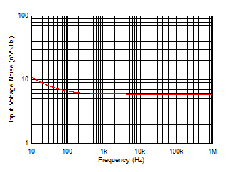
OPA863A OPA2863A Input Voltage Noise
                        Density vs Frequency
 
Figure 6-42 Input Voltage Noise Density vs Frequency
OPA863A OPA2863A Common-Mode Rejection
                        Ratio vs Frequency
 
Figure 6-44 Common-Mode Rejection Ratio vs Frequency
OPA863A OPA2863A Open-Loop Output Impedance
                        vs Frequency
 
Figure 6-46 Open-Loop Output Impedance vs Frequency
OPA863A OPA2863A Frequency Response vs
                        Supply Voltage
VOUT = 20 mVPP
Figure 6-41 Frequency Response vs Supply Voltage
OPA863A OPA2863A Input Current Noise
                        Density vs Frequency
 
Figure 6-43 Input Current Noise Density vs Frequency
OPA863A OPA2863A Power Supply Rejection
                        Ratio vs Frequency
 
Figure 6-45 Power Supply Rejection Ratio vs Frequency
OPA863A OPA2863A Crosstalk vs
                        Frequency
DSN package
Figure 6-47 Crosstalk vs Frequency