ZHCSF44A May   2016  – June 2016 OPT3002

PRODUCTION DATA.  

  1. 特性
  2. 应用
  3. 说明
  4. 修订历史记录
  5. Pin Configuration and Functions
  6. Specifications
    1. 6.1 Absolute Maximum Ratings
    2. 6.2 ESD Ratings
    3. 6.3 Recommended Operating Conditions
    4. 6.4 Thermal Information
    5. 6.5 Electrical Characteristics
    6. 6.6 Timing Requirements
    7. 6.7 Typical Characteristics
  7. Detailed Description
    1. 7.1 Overview
    2. 7.2 Functional Block Diagram
    3. 7.3 Feature Description
      1. 7.3.1 Automatic Full-Scale Range Setting
      2. 7.3.2 Interrupt Operation, INT Pin, and Interrupt Reporting Mechanisms
      3. 7.3.3 I2C Bus Overview
        1. 7.3.3.1 Serial Bus Address
        2. 7.3.3.2 Serial Interface
    4. 7.4 Device Functional Modes
      1. 7.4.1 Automatic Full-Scale Setting Mode
      2. 7.4.2 Interrupt Reporting Mechanism Modes
        1. 7.4.2.1 Latched Window-Style Comparison Mode
        2. 7.4.2.2 Transparent Hysteresis-Style Comparison Mode
        3. 7.4.2.3 End-of-Conversion Mode
        4. 7.4.2.4 End-of-Conversion and Transparent Hysteresis-Style Comparison Mode
    5. 7.5 Programming
      1. 7.5.1 Writing and Reading
        1. 7.5.1.1 High-Speed I2C Mode
        2. 7.5.1.2 General-Call Reset Command
        3. 7.5.1.3 SMBus Alert Response
    6. 7.6 Register Maps
      1. 7.6.1 Internal Registers
        1. 7.6.1.1 Register Descriptions
          1. 7.6.1.1.1 Result Register (address = 00h)
          2. 7.6.1.1.2 Configuration Register (address = 01h) [reset = C810h]
          3. 7.6.1.1.3 Low-Limit Register (address = 02h) [reset = C0000h]
          4. 7.6.1.1.4 High-Limit Register (address = 03h) [reset = BFFFh]
          5. 7.6.1.1.5 Manufacturer ID Register (address = 7Eh) [reset = 5449h]
  8. Application and Implementation
    1. 8.1 Application Information
      1. 8.1.1 Electrical Interface
      2. 8.1.2 Optical Interface
      3. 8.1.3 Compensation for the Spectral Response
    2. 8.2 Do's and Don'ts
  9. Power-Supply Recommendations
  10. 10Layout
    1. 10.1 Layout Guidelines
    2. 10.2 Layout Example
  11. 11器件和文档支持
    1. 11.1 文档支持
      1. 11.1.1 相关文档 
    2. 11.2 接收文档更新通知
    3. 11.3 社区资源
    4. 11.4 商标
    5. 11.5 静电放电警告
    6. 11.6 Glossary
  12. 12机械、封装和可订购信息
    1. 12.1 关于焊接和处理的相关建议
    2. 12.2 DNP (S-PDSO-N6) 机械制图

封装选项

机械数据 (封装 | 引脚)
散热焊盘机械数据 (封装 | 引脚)
订购信息

10 Layout

10.1 Layout Guidelines

The PCB layout design for the OPT3002 requires a couple of considerations. Bypass the power supply with a capacitor placed close to the OPT3002. Note that optically reflective surfaces of components also affect the performance of the design. The three-dimensional geometry of all components and structures around the sensor must be taken into consideration to prevent unexpected results from secondary optical reflections. Placing capacitors and components at a distance of at least twice the height of the component is usually sufficient. The most optimal optical layout is to place all close components on the opposite side of the PCB from the OPT3002. However, this approach may not be practical for the constraints of every design.

Electrically connecting the thermal pad to ground is recommended. This connection can be created either with a PCB trace or with vias to ground directly on the thermal pad itself. If the thermal pad contains vias, they are recommended to be of a small diameter (< 0.2 mm) to prevent them from wicking the solder away from the appropriate surfaces.

An example PCB layout with the OPT3002 is shown in Figure 24.

10.2 Layout Example
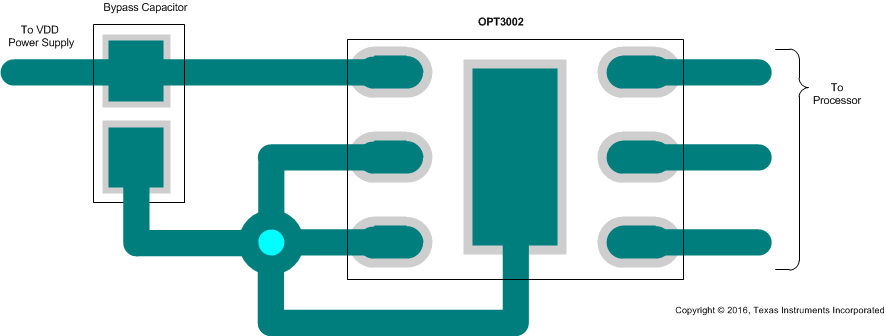
OPT3002 ai_layout_sbos745.gif Figure 24. Example PCB Layout with the OPT3002