At TA = 25°C, VDD = 3.3 V, 800-ms conversion time (CT = 1), automatic full-scale range (RN[3:0] = 1100b), white LED, and normal-angle incidence of light, unless otherwise specified.
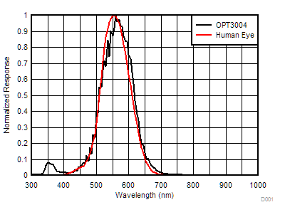 Figure 7-2 Spectral Response vs Wavelength
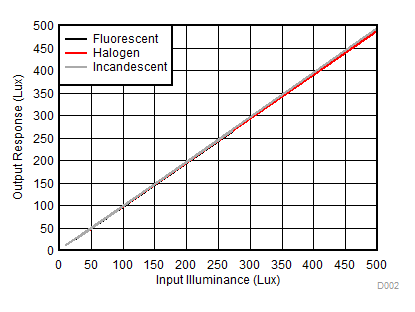 Figure 7-4 Output Response vs Input Illuminance, Multiple Light Sources (Fluorescent, Halogen, Incandescent)
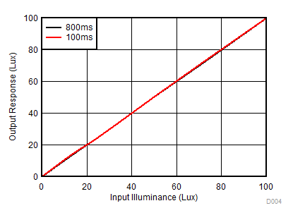 Figure 7-6 Output Response vs Input Illuminance (Mid Range = 0 lux to 100 lux)
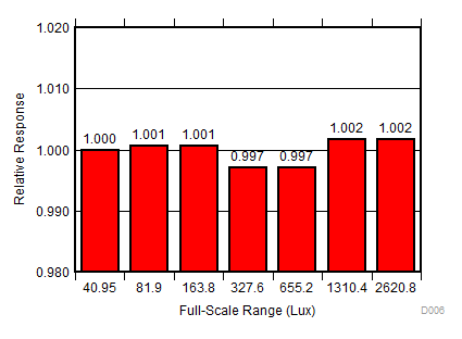
| Input illuminance = 33 lux, normalized to response of 40.95 lux full-scale |
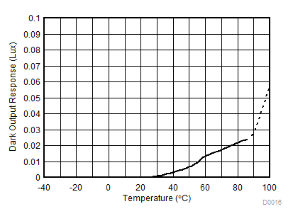 Figure 7-10 Dark Response vs Temperature
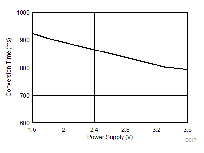 Figure 7-12 Conversion Time vs Power Supply
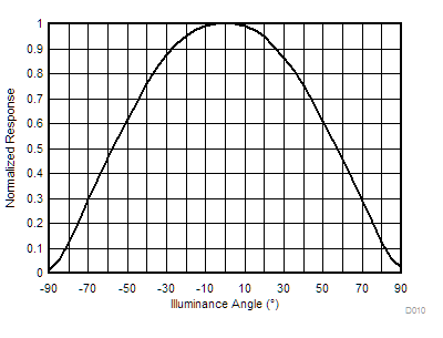 Figure 7-14 Normalized Response vs Illuminance Angle
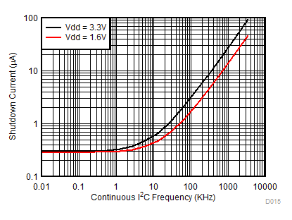
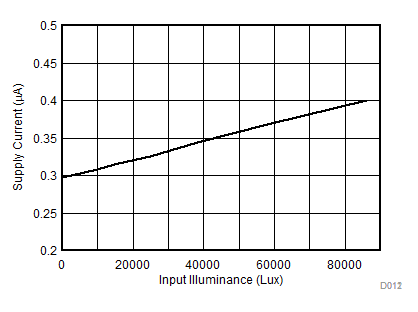 Figure 7-16 Shutdown Current vs Input Illuminance
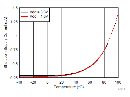
| M[1:0] = 00b, input illuminance = 0 lux |
|
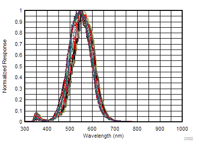 Figure 7-3 Spectral Response vs Wavelength from 85° to -85° in 10° Steps Normalized to each Angle of Incidence
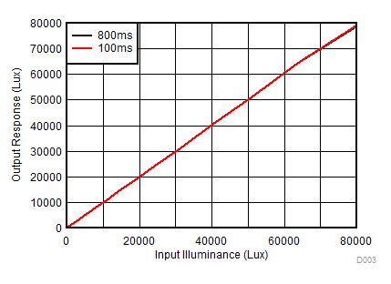 Figure 7-5 Output Response vs Input Illuminance (Entire Range = 0 lux to 83k lux)
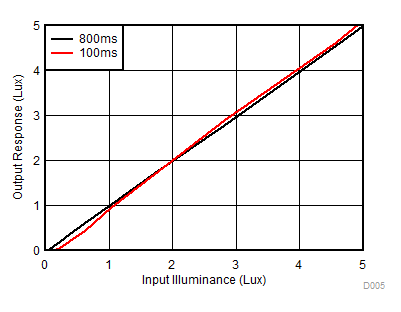 Figure 7-7 Output Response vs Input Illuminance (Low Range = 0 lux to 5 lux)
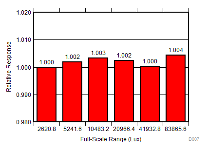
| Input illuminance = 2490 lux, normalized to response of 2620.8 lux full-scale |
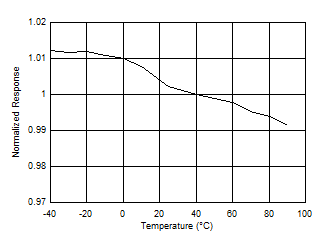 Figure 7-11 Normalized Response vs Temperature
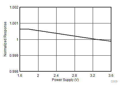 Figure 7-13 Normalized Response vs Power-Supply Voltage
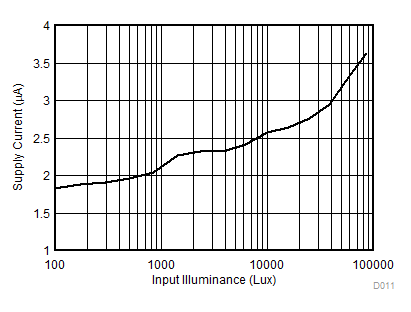
 Figure 7-15 Supply Current vs Input Illuminance
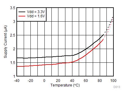
 Figure 7-17 Supply Current vs Temperature
| Input illuminance = 80 lux, SCL = SDA, continuously toggled at I2C frequency Note: A typical application runs at a lower duty cycle and thus consumes a lower current. |
 Figure 7-2 Spectral Response vs Wavelength
 Figure 7-4 Output Response vs Input Illuminance, Multiple Light Sources (Fluorescent, Halogen, Incandescent)
 Figure 7-6 Output Response vs Input Illuminance (Mid Range = 0 lux to 100 lux)
 Figure 7-10 Dark Response vs Temperature
 Figure 7-12 Conversion Time vs Power Supply


 Figure 7-3 Spectral Response vs Wavelength from 85° to -85° in 10° Steps Normalized to each Angle of Incidence
 Figure 7-5 Output Response vs Input Illuminance (Entire Range = 0 lux to 83k lux)
 Figure 7-7 Output Response vs Input Illuminance (Low Range = 0 lux to 5 lux)
 Figure 7-11 Normalized Response vs Temperature
 Figure 7-13 Normalized Response vs Power-Supply Voltage