ZHCSFL9 October 2016 OPT3006
PRODUCTION DATA.
- 1 特性
- 2 应用
- 3 说明
- 4 修订历史记录
- 5 Pin Configuration and Functions
- 6 Specifications
-
7 Detailed Description
- 7.1 Overview
- 7.2 Functional Block Diagram
- 7.3 Feature Description
- 7.4 Device Functional Modes
- 7.5 Programming
- 7.6
Register Maps
- 7.6.1
Internal Registers
- 7.6.1.1
Register Descriptions
- 7.6.1.1.1 Result Register (offset = 00h)
- 7.6.1.1.2 Configuration Register (offset = 01h) [reset = C810h]
- 7.6.1.1.3 Low-Limit Register (offset = 02h) [reset = C0000h]
- 7.6.1.1.4 High-Limit Register (offset = 03h) [reset = BFFFh]
- 7.6.1.1.5 Manufacturer ID Register (offset = 7Eh) [reset = 5449h]
- 7.6.1.1.6 Device ID Register (offset = 7Fh) [reset = 3001h]
- 7.6.1.1
Register Descriptions
- 7.6.1
Internal Registers
- 8 Application and Implementation
- 9 Power-Supply Recommendations
- 10Layout
- 11器件和文档支持
- 12机械、封装和可订购信息
6 Specifications
6.1 Absolute Maximum Ratings(1)
| MIN | MAX | UNIT | ||
|---|---|---|---|---|
| Voltage | VDD to GND | –0.5 | 6 | V |
| SDA, SCL, INT, and ADDR to GND | –0.5 | 6 | V | |
| Current into any pin | 10 | mA | ||
| Temperature | Junction | 150 | °C | |
| Storage, Tstg | –65 | 150(2) | °C | |
(1) Stresses beyond those listed under Absolute Maximum Ratings may cause permanent damage to the device. These are stress ratings only, and do not imply functional operation of the device at these or any other conditions beyond those indicated under Recommended Operating Conditions. Exposure to absolute-maximum-rated conditions for extended periods may affect device reliability.
(2) Long exposure to temperatures higher than 105°C can cause package discoloration, spectral distortion, and measurement inaccuracy.
6.2 ESD Ratings
| VALUE | UNIT | |||
|---|---|---|---|---|
| V(ESD) | Electrostatic discharge | Human-body model (HBM), per ANSI/ESDA/JEDEC JS-001(1) | ±2000 | V |
| Charged-device model (CDM), per JEDEC specification JESD22-C101(2) | ±500 | |||
(1) JEDEC document JEP155 states that 500-V HBM allows safe manufacturing with a standard ESD control process.
(2) JEDEC document JEP157 states that 250-V CDM allows safe manufacturing with a standard ESD control process.
6.3 Recommended Operating Conditions
| MIN | NOM | MAX | UNIT | ||
|---|---|---|---|---|---|
| Operating temperature | –40 | 85 | °C | ||
| Operating power-supply voltage | 1.6 | 3.6 | V | ||
6.4 Thermal Information
| THERMAL METRIC(1) | OPT3006 | UNIT | |
|---|---|---|---|
| YMF (PicoStar) | |||
| 6 PINS | |||
| RθJA | Junction-to-ambient thermal resistance | 122.8 | °C/W |
| RθJC(top) | Junction-to-case (top) thermal resistance | 1.4 | °C/W |
| RθJB | Junction-to-board thermal resistance | 34.9 | °C/W |
| ψJT | Junction-to-top characterization parameter | 0.8 | °C/W |
| ψJB | Junction-to-board characterization parameter | 35.3 | °C/W |
(1) For more information about traditional and new thermal metrics, see the Semiconductor and IC Package Thermal Metrics application report.
6.5 Electrical Characteristics
At TA = 25°C, VDD = 3.3 V, 800-ms conversion time (CT = 1)(2), automatic full-scale range (RN[3:0] = 1100b(2)), white LED, and normal-angle incidence of light, unless otherwise specified.| PARAMETER | TEST CONDITIONS | MIN | TYP | MAX | UNIT | ||
|---|---|---|---|---|---|---|---|
| OPTICAL | |||||||
| Peak irradiance spectral responsivity | 550 | nm | |||||
| Resolution (LSB) | Lowest full-scale range, RN[3:0] = 0000b(2) | 0.01 | lux | ||||
| Full-scale illuminance | 83865.6 | lux | |||||
| Measurement output result | 0.64 lux per ADC code, 2620.80 lux full-scale (RN[3:0] = 0110)(2), 2000 lux input(3) | 2500 | 3125 | 3750 | ADC codes | ||
| 1600 | 2000 | 2400 | lux | ||||
| Relative accuracy between gain ranges(1) | 0.2% | ||||||
| Infrared response (850 nm)(3) | 0.2% | ||||||
| Light source variation (incandescent, halogen, fluorescent) |
Bare device, no cover glass | 4% | |||||
| Linearity | Input illuminance > 40 lux | 2% | |||||
| Input illuminance < 40 lux | 5% | ||||||
| Measurement drift across temperature | Input illuminance = 2000 lux | 0.01 | %/°C | ||||
| Dark condition, ADC output | 0.01 lux per ADC code | 0 | 3 | ADC codes | |||
| 0 | 0.03 | lux | |||||
| Half-power angle | 50% of full-power reading | 44 | degrees | ||||
| PSRR | Power-supply rejection ratio | VDD at 3.6 V and 1.6 V | 0.1 | %/V(4) | |||
| POWER SUPPLY | |||||||
| VDD | Operating range | 1.6 | 3.6 | V | |||
| VI²C | Operating range of I2C pull-up resistor | I2C pull-up resistor, VDD ≤ VI²C | 1.6 | 5.5 | V | ||
| IQ | Quiescent current | Dark | Active, VDD = 3.6 V | 1.8 | 2.5 | µA | |
| Shutdown (M[1:0] = 00)(2), VDD = 3.6 V | 0.3 | 0.47 | µA | ||||
| Full-scale lux | Active, VDD = 3.6 V | 3.7 | µA | ||||
| Shutdown, (M[1:0] = 00)(2) |
0.4 | µA | |||||
| POR | Power-on-reset threshold | TA = 25°C | 0.8 | V | |||
| DIGITAL | |||||||
| I/O pin capacitance | 3 | pF | |||||
| Total integration time(5) | (CT = 1)(2), 800-ms mode, fixed lux range | 720 | 800 | 880 | ms | ||
| (CT = 0)(2), 100-ms mode, fixed lux range | 90 | 100 | 110 | ms | |||
| VIL | Low-level input voltage (SDA, SCL, and ADDR) |
0 | 0.3 × VDD | V | |||
| VIH | High-level input voltage (SDA, SCL, and ADDR) |
0.7 × VDD | 5.5 | V | |||
| IIL | Low-level input current (SDA, SCL, and ADDR) |
0.01 | 0.25(6) | µA | |||
| VOL | Low-level output voltage (SDA and INT) |
IOL= 3 mA | 0.32 | V | |||
| IZH | Output logic high, high-Z leakage current (SDA, INT) | Pin at VDD | 0.01 | 0.25(6) | µA | ||
| TEMPERATURE | |||||||
| Specified temperature range | –40 | 85 | °C | ||||
(1) Characterized by measuring fixed near-full-scale light levels on the higher adjacent full-scale range setting.
(2) Refers to a control field within the configuration register.
(3) Tested with the white LED calibrated to 2k lux and an 850-nm LED.
(4) PSRR is the percent change of the measured lux output from its current value, divided by the change in power supply voltage, as characterized by results from 3.6-V and 1.6-V power supplies.
(5) The conversion time, from start of conversion until the data are ready to be read, is the integration time plus 3 ms.
(6) The specified leakage current is dominated by the production test equipment limitations. Typical values are much smaller.
6.6 Timing Requirements(1)
| MIN | TYP | MAX | UNIT | ||
|---|---|---|---|---|---|
| I2C FAST MODE | |||||
| fSCL | SCL operating frequency | 0.01 | 0.4 | MHz | |
| tBUF | Bus free time between stop and start | 1300 | ns | ||
| tHDSTA | Hold time after repeated start | 600 | ns | ||
| tSUSTA | Setup time for repeated start | 600 | ns | ||
| tSUSTO | Setup time for stop | 600 | ns | ||
| tHDDAT | Data hold time | 20 | 900 | ns | |
| tSUDAT | Data setup time | 100 | ns | ||
| tLOW | SCL clock low period | 1300 | ns | ||
| tHIGH | SCL clock high period | 600 | ns | ||
| tRC and tFC | Clock rise and fall time | 300 | ns | ||
| tRD and tFD | Data rise and fall time | 300 | ns | ||
| tTIMEO | Bus timeout period. If the SCL line is held low for this duration of time, the bus state machine is reset. | 28 | ms | ||
| I2C HIGH-SPEED MODE | |||||
| fSCL | SCL operating frequency | 0.01 | 2.6 | MHz | |
| tBUF | Bus free time between stop and start | 160 | ns | ||
| tHDSTA | Hold time after repeated start | 160 | ns | ||
| tSUSTA | Setup time for repeated start | 160 | ns | ||
| tSUSTO | Setup time for stop | 160 | ns | ||
| tHDDAT | Data hold time | 20 | 140 | ns | |
| tSUDAT | Data setup time | 20 | ns | ||
| tLOW | SCL clock low period | 240 | ns | ||
| tHIGH | SCL clock high period | 60 | ns | ||
| tRC and tFC | Clock rise and fall time | 40 | ns | ||
| tRD and tFD | Data rise and fall time | 80 | ns | ||
| tTIMEO | Bus timeout period. If the SCL line is held low for this duration of time, the bus state machine is reset. | 28 | ms | ||
(1) All timing parameters are referenced to low and high voltage thresholds of 30% and 70%, respectively, of final settled value.
 Figure 1. I2C Detailed Timing Diagram
6.7 Typical Characteristics
At TA = 25°C, VDD = 3.3 V, 800-ms conversion time (CT = 1), automatic full-scale range (RN[3:0] = 1100b), white LED, and normal-angle incidence of light, unless otherwise specified.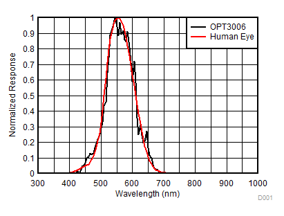
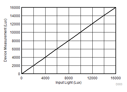
(Higher Range = 0 lux to 16k lux)
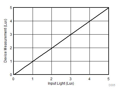
(Low Range = 0 lux to 5 lux)
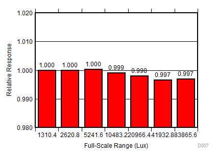
| Input illuminance = 960 lux, normalized to response of 2560 lux full-scale |
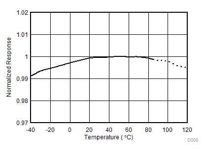
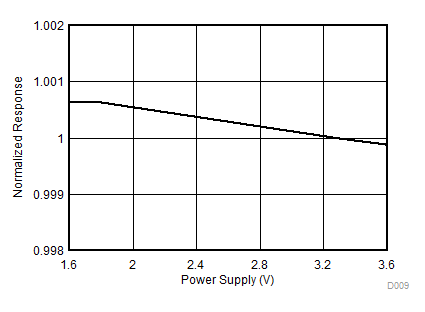
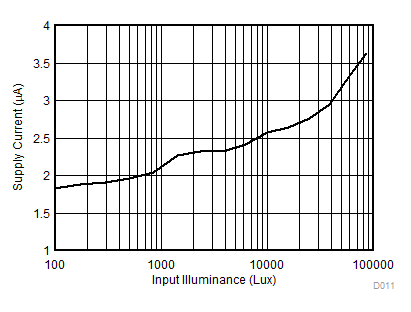
| M[1:0] = 10b |
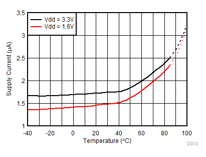
| M[1:0] = 10b |
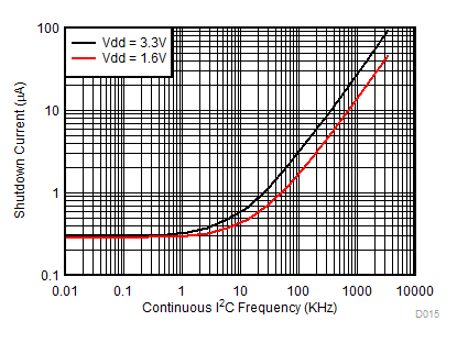
| Input illuminance = 80 lux, SCL = SDA, continuously toggled at I2C frequency Note: A typical application runs at a lower duty cycle and thus consumes a lower current. |
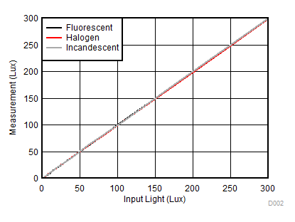
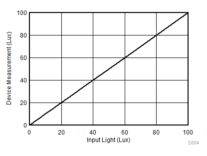
(Mid Range = 0 lux to 100 lux)
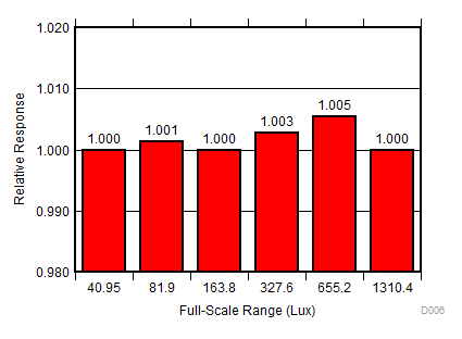
| Input illuminance = 30 lux, normalized to response of 40.95 lux full-scale |
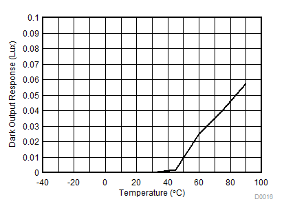
| Average of 30 devices | ||
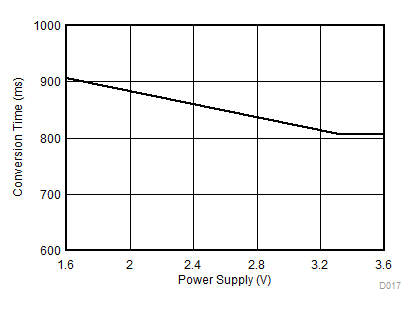
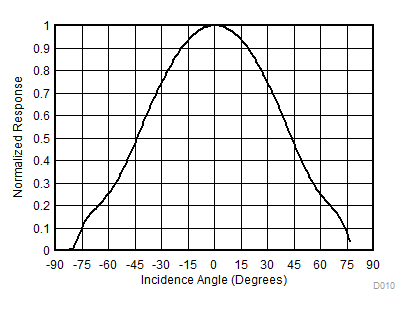
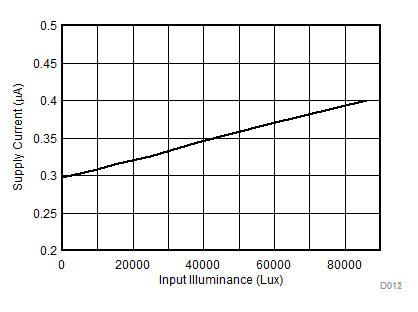
| M[1:0] = 00b |
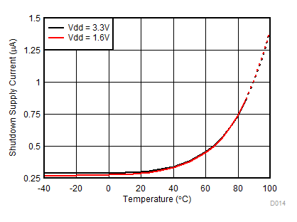
| M[1:0] = 00b, input illuminance = 0 lux |