ZHCSPI9A December 2021 – December 2022 OPT4001
PRODUCTION DATA
- 1 特性
- 2 应用
- 3 说明
- 4 Revision History
- 5 说明(续)
- 6 Pin Configuration and Functions
- 7 Specifications
- 8 Detailed Description
- 9 Application and Implementation
- 10Device and Documentation Support
- 11Mechanical, Packaging, and Orderable Information
9.2.1.2.1 Optomechanical Design (PicoStar Variant)
After completing the electrical design and understanding optical interface, the next task is the optomechanical design of the FPCB cutout. Design this cutout in conjunction with the tolerance capabilities of the FPCB manufacturer. Or, conversely, choose the FPCB manufacturer for the capabilities of creating this cutout. A semi-rectangular shape of the cutout, created with a standard FPCB laser, is presented here. There are many alternate approaches with different cost, tolerance, and performance tradeoffs.
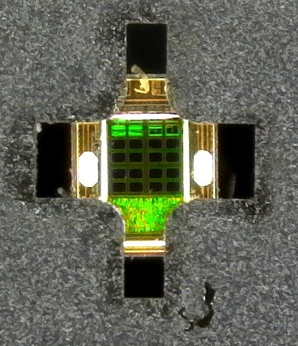
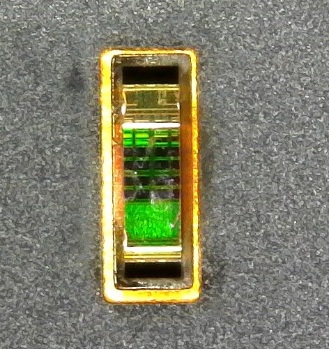
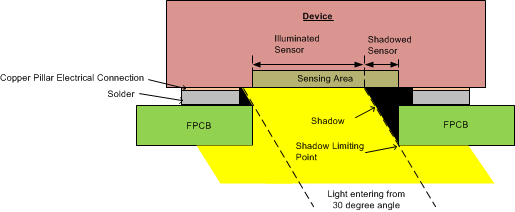
An image of the created FPCB with the plus shaped cutout and a rectangular shaped cutout is shown below. The plus shape is a good choice for light collection in both directions with a wider field of view. In case of the rectangular cutout shape, the long (vertical) direction of the cutout has minimal effect on the angular response because any shadows created from the FPCB do not come near the sensor. The long cutout direction defines the axis of rotation with the less restricted field of view. The narrow (horizontal) direction of the cutout, which is limited by the electrical connections to OPT4001, can create shadows that can have a minor impact on the angular response. The narrow cutout direction defines the axis of rotation of the more restricted view. The possibility of shadows are illustrated in Figure 9-6, a cross-sectional diagram showing the OPT4001 device, with the sensing area, so ldered to the FPCB with the cutout. A circular cutout is more restrictive in the field of view casting shadow from all directions of light. TI recommends to take in to account the effect of shadows and impact of this on the field of view of the sensor. The product folder has application notes and tools to help understand these artifacts.
 Figure 9-4 Image of
FPCB With OPT4001 Mounted, Receiving Light Through
the Cutout with a Plus Shape
 Figure 9-5 Image of
FPCB With OPT4001 Mounted, Receiving Light Through
the Cutout with a Rectangular Shape
 Figure 9-6 Cross-Sectional Diagram
of OPT4001 Soldered to an FPCB With a Cutout,
Including Light Entering From an Angle
Figure 9-6 Cross-Sectional Diagram
of OPT4001 Soldered to an FPCB With a Cutout,
Including Light Entering From an AngleThere can be an additional need to put a product casing over the assembly of the device and the FPCB. The window sizing and placement for such an assembly is discussed in more rigorous detail in application report OPT3001: Ambient Light Sensor Application Guide (SBEA002).