ZHCSE82B June 2015 – October 2015 OPT8241
PRODUCTION DATA.
- 1 特性
- 2 应用
- 3 说明
- 4 修订历史记录
- 5 Pin Configuration and Functions
- 6 Specifications
- 7 Detailed Description
- 8 Application and Implementation
- 9 Power Supply Recommendations
- 10Layout
- 11器件和文档支持
- 12机械、封装和可订购信息
6 Specifications
6.1 Absolute Maximum Ratings
over operating free-air temperature range (unless otherwise noted)(1)| MIN | MAX | UNIT | ||
|---|---|---|---|---|
| IOVDD | Digital I/O supply | –0.3 | 4.0 | V |
| AVDDH | Analog supply | –0.3 | 4.0 | V |
| DVDDH | Digital I/O supply | –0.3 | 4.0 | V |
| PVDD | Pixel supply | –0.3 | 4.0 | V |
| AVDD | Analog supply | –0.3 | 2.2 | V |
| VMIXH | Mix supply | –0.3 | 2.5 | V |
| DVDD | Digital supply | –0.3 | 2.2 | V |
| AVDD_PLL | PLL supply | –0.3 | 2.2 | V |
| VI | Input voltage at input pins | –0.3 | VCC + 0.3(2) | V |
| TJ | Operating junction temperature | 0 | 125 | °C |
| Tstg | Storage temperature | –40 | 125 | °C |
(1) Stresses beyond those listed under Absolute Maximum Ratings may cause permanent damage to the device. These are stress ratings only, which do not imply functional operation of the device at these or any other conditions beyond those indicated under Recommended Operating Conditions. Exposure to absolute-maximum-rated conditions for extended periods may affect device reliability.
(2) VCC refers to the I/O bank voltage.
6.2 ESD Ratings
| VALUE | UNIT | |||
|---|---|---|---|---|
| V(ESD) | Electrostatic discharge | Human-body model (HBM), per ANSI/ESDA/JEDEC JS-001(1) | ±1000 | V |
| Charged-device model (CDM), per JEDEC specification JESD22-C101(2) | ±250 | |||
(1) JEDEC document JEP155 states that 500-V HBM allows safe manufacturing with a standard ESD control process.
(2) JEDEC document JEP157 states that 250-V CDM allows safe manufacturing with a standard ESD control process.
6.3 Recommended Operating Conditions
over operating free-air temperature range (unless otherwise noted)| MIN | NOM | MAX | UNIT | ||
|---|---|---|---|---|---|
| IOVDD | Digital I/O supply | 1.7 | 1.8 to 3.3 | 3.6 | V |
| AVDDH | Analog supply | 3.0 | 3.3 | 3.6 | V |
| DVDDH | Digital I/O supply | 3.0 | 3.3 | 3.6 | V |
| PVDD | Pixel supply | 3.0 | 3.3 | 3.6 | V |
| AVDD | Analog supply | 1.7 | 1.8 | 1.9 | V |
| VMIXH | Mix supply | 1.4 | 1.5 | 2.0 | V |
| DVDD | Digital supply | 1.7 | 1.8 | 1.9 | V |
| AVDD_PLL | PLL supply | 1.7 | 1.8 | 1.9 | V |
| TA | Operating ambient temperature | 0 | 70 | °C | |
6.4 Thermal Information
| THERMAL METRIC(1) | OPT8241 | UNIT | ||
|---|---|---|---|---|
| NBN (COG) | ||||
| 78 PINS | ||||
| RθJA | Junction-to-ambient thermal resistance | Without underfill | 79.2 | °C/W |
| With underfill | 41.0 | °C/W | ||
| RθJC(top) | Junction-to-case (top) thermal resistance | 18.6 | °C/W | |
| RθJB | Junction-to-board thermal resistance | 51.0 | °C/W | |
| ψJT | Junction-to-top characterization parameter | 6.3 | °C/W | |
| ψJB | Junction-to-board characterization parameter | 51.1 | °C/W | |
| RθJC(bot) | Junction-to-case (bottom) thermal resistance | 18.6 | °C/W | |
(1) For more information about traditional and new thermal metrics, see the IC Package Thermal Metrics application report, SPRA953.
6.5 Electrical Characteristics
All specifications at TA = 25°C, VAVDDH = 3.3 V, VAVDD = 1.8 V, VVMIXH = 1.5 V, VDVDD = 1.8 V, VDVDDH = 3.3 V, VPVDD = 3.3 V, VSUB_BIAS = 0 V, integration duty cycle = 10%, system clock frequency = 48 MHz, modulation frequency = 50 MHz, and 850 nm illumination, unless otherwise noted.| PARAMETER | TEST CONDITIONS | MIN | TYP | MAX | UNIT | |
|---|---|---|---|---|---|---|
| SENSOR | ||||||
| V | Maximum rows | 240 | Rows | |||
| H | Maximum columns | 320 | Columns | |||
| PP | Pixel pitch | 15 | μm | |||
| POWER (Normal Operation) | ||||||
| IAVDD_PLL | PLL supply current | 9 | mA | |||
| IAVDD | Analog supply current | Without dynamic power-down | 40 | mA | ||
| With dynamic power-down | 20 | |||||
| IDVDDH | 3.3-V digital supply current | 5 | mA | |||
| IAVDDH | 3.3-V analog supply current | Without dynamic power-down | 17 | mA | ||
| With dynamic power-down | 7 | |||||
| IPVDD | Pixel VDD current | 2 | mA | |||
| IVMIXH | Demodulation current | 10% integration duty cycle | 70 | mA | ||
| 100% integration duty cycle | 600 | |||||
| IIOVDD | I/O supply current (CMOS mode) | 20 | mA | |||
| I/O supply current (LVDS mode) | 2 | |||||
| IDVDD | Digital supply current | 45 | mA | |||
| POWER (Standby) | ||||||
| IIOVDD | I/O supply current | 0.7 | mA | |||
| IAVDD_PLL | PLL supply current | 0.3 | mA | |||
| IAVDD | Analog supply current | 0.3 | mA | |||
| IDVDD | Digital supply current | 0.6 | mA | |||
| IDVDDH | 3.3-V digital supply current | 1.1 | mA | |||
| IAVDDH | 3.3-V analog supply current | 0.2 | mA | |||
| IVMIXH | Demodulation current | 0 | mA | |||
| IPVDD | Pixel VDD current | 0 | mA | |||
| CMOS I/Os | ||||||
| VIH | Input high-level threshold | 0.7 × VCC(1) | V | |||
| VIL | Input low-level threshold | 0.3 × VCC(1) | V | |||
| VOH | Output high level | IOH = –2 mA | VCC(1) – 0.45 | V | ||
| IOH = –8 mA | VCC(1) – 0.5 | |||||
| VOL | Output Low Level | IOL = 2 mA | 0.35 | V | ||
| IOL = 8 mA | 0.65 | |||||
| II | Input pin leakage current | Pins with pullup, pulldown resistor | ±50 | µA | ||
| Pins without pullup, pulldown resistor | ±10 | |||||
| CI | Input capacitance | 5 | pF | |||
| IOH | Output current | 10 | mA | |||
| IOL | 10 | |||||
(1) VCC is equal to IOVDD or DVDDH, based on the I/O bank listed in the Pin Functions table.
6.6 Timing Requirements
| MIN | NOM | MAX | UNIT | ||
|---|---|---|---|---|---|
| MCLK duty cycle | 48% | 52% | |||
| MCLK frequency | 12 | 50 | MHz | ||
| VD_IN pulse duration | 2 × MCLK period | ns | |||
| RTSZ low pulse duration (reset) | 100 | ns | |||
6.7 Switching Characteristics
over operating free-air temperature range (unless otherwise noted); VDVDD = 1.8 V, VDVDDH = 3.3 V, and VIOVDD = 1.8 V| PARAMETER | TEST CONDITIONS | MIN | TYP | MAX | UNIT | |
|---|---|---|---|---|---|---|
| DDR LVDS MODE | ||||||
| tSU | Data setup time | Data valid to zero crossing of DCLKP, DCLKM | 0.48 | ns | ||
| tH | Data hold time | Zero crossing of DCLKP, DCLKM to data becoming invalid | 0.54 | ns | ||
| tFALL, tRISE | Data fall time, data rise time | Rise time measured from –100 mV to +100 mV | 0.35 | ns | ||
| tCLKRISE, tCLKFALL | Output clock rise time, output clock fall time |
Rise time measured from –100 mV to +100 mV | 0.35 | ns | ||
| PARALLEL CMOS MODE | ||||||
| tSU | Data setup time | Data valid to zero crossing of CLKOUT | 1.5 | ns | ||
| tH | Data hold time | Zero crossing of CLKOUT to data becoming invalid | 3.5 | ns | ||
| tFALL, tRISE | Data fall time, data rise time | Rise time measured from 30% to 70% of IOVDD | 2.5 | ns | ||
| tCLKRISE, tCLKFALL | Output clock rise time, output clock fall time |
Rise time measured from 30% to 70% of IOVDD | 2.2 | ns | ||
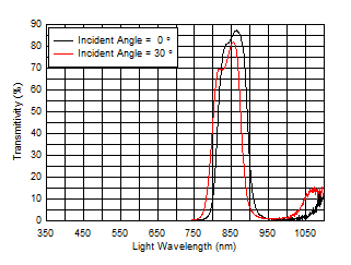
6.8 Optical Characteristics
over operating free-air temperature range (unless otherwise noted)| PARAMETER | TEST CONDITIONS | MIN | TYP | MAX | UNIT | |
|---|---|---|---|---|---|---|
| Glass side | Top | Side | ||||
| Passband (50% relative transmittance(1)) |
0° incident angle | 813 to 893 | nm | |||
| 30° incident angle | 798 to 877 | nm | ||||
| Passband (90% relative transmittance(1)) |
0° incident angle | 830 to 881 | nm | |||
| 30° incident angle | 838 to 867 | nm | ||||
| AOI | Recommended angle of incidence | 0 | 35 | Degrees | ||
| Maximum absolute transmittance | 0° incident angle | 87.34% at 863 | nm | |||
| 30° incident angle | 81.89% at 855 | nm | ||||
(1) Relative transmittance is a ratio of transmittance to maximum absolute transmittance at the same angle of incidence.

1. Dn = bits D0, D2, D4, and so forth. Dn+1 = bits D1, D3, D5, and so forth.
Figure 1. LVDS Switching Diagram

1. Dn = bits D0, D1, D2, and so forth.
Figure 2. CMOS Switching Diagram
6.9 Typical Characteristics
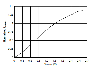
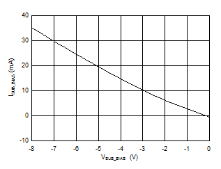
At VAVDDH = 3.3 V, VAVDD = 1.8 V, VVMIXH = 1.5 V, VDVDD = 1.8 V, VDVDDH = 3.3 V, VPVDD = 3.3 V, VSUB_BIAS = 0 V, and integration duty cycle = 10%, unless otherwise noted.
| Normalized to VMIXH = 1.5 V |
VMIXH Supply Voltage

Light Wavelength

VSUB_BIAS Supply Voltage