SCPS145B December 2007 – February 2016 P82B715
PRODUCTION DATA.
- 1 Features
- 2 Applications
- 3 Description
- 4 Revision History
- 5 Pin Configuration and Functions
- 6 Specifications
- 7 Parameter Measurement Information
- 8 Detailed Description
- 9 Application and Implementation
- 10Power Supply Recommendations
- 11Layout
- 12Device and Documentation Support
- 13Mechanical, Packaging, and Orderable Information
11 Layout
11.1 Layout Guidelines
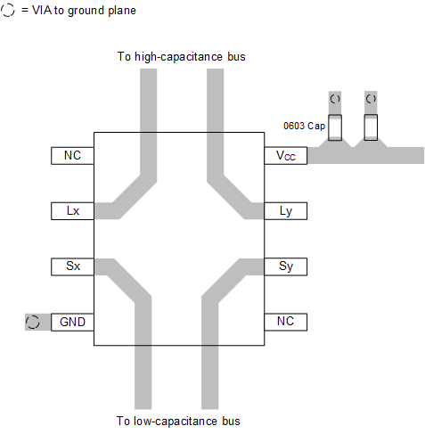
General layout best practices are recommended. It is common to have a dedicated ground plane on an inner layer of the board, and pins that are connected to ground must have a low-impedance path to the ground place in the form of wide polygon pours, and multiple vias.
Bypass and decoupling capacitors are commonly used to control the voltage on the VCC pin, using a larger capacitor to provide additional power in the event of a short power supply glitch (typically 1 μF), and a smaller capacitor (typically 0.1 μF) to filter out high-frequency ripple.
11.2 Layout Example
 Figure 8. D Package Example Layout