ZHCSQD8C July 2007 – April 2022 PCA9306-Q1
PRODUCTION DATA
- 1 特性
- 2 应用
- 3 说明
- 4 Revision History
- 5 说明(续)
- 6 Pin Configuration and Functions
-
7 Specifications
- 7.1 Absolute Maximum Ratings
- 7.2 ESD Ratings
- 7.3 Recommended Operating Conditions
- 7.4 Thermal Information
- 7.5 Electrical Characteristics
- 7.6 Switching Characteristics: Translating Down, VIH = 3.3 V
- 7.7 Switching Characteristics: Translating Down, VIH = 2.5 V
- 7.8 Switching Characteristics: Translating Up, VIH = 2.3 V
- 7.9 Switching Characteristics: Translating Up, VIH = 1.5 V
- 7.10 Typical Characteristics
- 8 Parameter Measurement Information
-
9 Detailed Description
- 9.1
Overview
- 9.1.1 Definition of threshold voltage
- 9.1.2 Correct Device Set Up
- 9.1.3 Disconnecting a Target from the Main I2C Bus Using the EN Pin
- 9.1.4 Supporting Remote Board Insertion to Backplane with PCA9306-Q1
- 9.1.5 Switch Configuration
- 9.1.6 Controller on Side 1 or Side 2 of Device
- 9.1.7 LDO and PCA9306-Q1 Concerns
- 9.1.8 Current Limiting Resistance on VREF2
- 9.2 Functional Block Diagram
- 9.3 Feature Description
- 9.4 Device Functional Modes
- 9.1
Overview
- 10Application and Implementation
- 11Power Supply Recommendations
- 12Layout
- 13Device and Documentation Support
- 14Mechanical, Packaging, and Orderable Information
9.1.3 Disconnecting a Target from the Main I2C Bus Using the EN Pin
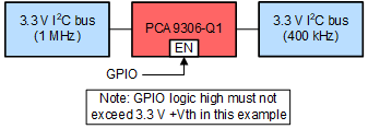
PCA9306-Q1 can be used as a switch to disconnect one side of the device from the main I2C bus. This can be advantageous in multiple situations. One instance of this situation is if there are devices on the I2C bus which only supports fast mode (400 kHz) while other devices on the bus support fast mode plus (1 MHz). An example of this is displayed in Figure 9-3.
 Figure 9-3 Example of an I2C bus with multiple supported frequencies
In this situation, if the controller is on the 1 MHz side then communicating at 1 MHz should not be attempted if PCA9306-Q1 were enabled. It needs to be disabled for PCA9306-Q1 to avoid possibly glitching state machines in devices which were designed to operate correctly at 400 kHz or slower. When PCA9306-Q1 is disabled, the controller can communicate with the 1 MHz devices without disturbing the 400 kHz bus. When the PCA9306-Q1 is enabled, communication across both sides at 400 kHz is acceptable.