ZHCSQD8C July 2007 – April 2022 PCA9306-Q1
PRODUCTION DATA
- 1 特性
- 2 应用
- 3 说明
- 4 Revision History
- 5 说明(续)
- 6 Pin Configuration and Functions
-
7 Specifications
- 7.1 Absolute Maximum Ratings
- 7.2 ESD Ratings
- 7.3 Recommended Operating Conditions
- 7.4 Thermal Information
- 7.5 Electrical Characteristics
- 7.6 Switching Characteristics: Translating Down, VIH = 3.3 V
- 7.7 Switching Characteristics: Translating Down, VIH = 2.5 V
- 7.8 Switching Characteristics: Translating Up, VIH = 2.3 V
- 7.9 Switching Characteristics: Translating Up, VIH = 1.5 V
- 7.10 Typical Characteristics
- 8 Parameter Measurement Information
-
9 Detailed Description
- 9.1
Overview
- 9.1.1 Definition of threshold voltage
- 9.1.2 Correct Device Set Up
- 9.1.3 Disconnecting a Target from the Main I2C Bus Using the EN Pin
- 9.1.4 Supporting Remote Board Insertion to Backplane with PCA9306-Q1
- 9.1.5 Switch Configuration
- 9.1.6 Controller on Side 1 or Side 2 of Device
- 9.1.7 LDO and PCA9306-Q1 Concerns
- 9.1.8 Current Limiting Resistance on VREF2
- 9.2 Functional Block Diagram
- 9.3 Feature Description
- 9.4 Device Functional Modes
- 9.1
Overview
- 10Application and Implementation
- 11Power Supply Recommendations
- 12Layout
- 13Device and Documentation Support
- 14Mechanical, Packaging, and Orderable Information
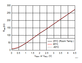
7.10 Typical Characteristics

| VEN = 1.5 V | II = 15 mA | |
| VEN = 4.5 V | II = 15 mA | |