ZHCS780B March 2012 – March 2016 PCA9515B
PRODUCTION DATA.
6 Specifications
6.1 Absolute Maximum Ratings
over operating free-air temperature range (unless otherwise noted) (1)| MIN | MAX | UNIT | |||
|---|---|---|---|---|---|
| VCC | Supply voltage | –0.5 | 7 | V | |
| VI | Enable input voltage (2) | –0.5 | 7 | V | |
| VI/O | I2C bus voltage(2) | –0.5 | 7 | V | |
| IIK | Input clamp current | VI < 0 | –50 | mA | |
| IOK | Output clamp current | VO < 0 | –50 | mA | |
| IO | Continuous output current | ±50 | mA | ||
| Continuous current through VCC or GND | ±100 | mA | |||
| Tstg | Storage temperature | –65 | 150 | °C | |
(1) Stresses beyond those listed under Absolute Maximum Ratings may cause permanent damage to the device. These are stress ratings only, which do not imply functional operation of the device at these or any other conditions beyond those indicated under Recommended Operating Conditions. Exposure to absolute-maximum-rated conditions for extended periods may affect device reliability.
(2) The input negative-voltage and output voltage ratings may be exceeded if the input and output current ratings are observed.
6.2 ESD Ratings
| VALUE | UNIT | |||
|---|---|---|---|---|
| V(ESD) | Electrostatic discharge | Human-body model (HBM), per ANSI/ESDA/JEDEC JS-001(1) | ±2000 | V |
| Charged-device model (CDM), per JEDEC specification JESD22-C101(2) | ±1000 | |||
(1) JEDEC document JEP155 states that 500-V HBM allows safe manufacturing with a standard ESD control process.
(2) JEDEC document JEP157 states that 250-V CDM allows safe manufacturing with a standard ESD control process.
6.3 Recommended Operating Conditions
| MIN | MAX | UNIT | |||
|---|---|---|---|---|---|
| VCC | Supply voltage | 2.3 | 3.6 | V | |
| VIH | High-level input voltage | SDA and SCL inputs | 0.7 × VCC | 5.5 | V |
| EN input | 2 | 5.5 | |||
| VIL (1) | Low-level input voltage | SDA and SCL inputs | –0.5 | 0.3 × VCC | V |
| EN input | –0.5 | 0.8 | |||
| VILc (1) | SDA and SCL low-level input voltage contention | –0.5 | 0.4 | V | |
| IOL | Low-level output current | VCC = 2.3 V | 6 | mA | |
| VCC = 3 V | 6 | ||||
| TA | Operating free-air temperature | –40 | 85 | °C | |
(1) VIL specification is for the EN input and the first low level seen by the SDAx and SCLx lines. VILc is for the second and subsequent low levels seen by the SDAx and SCLx lines. VILc must be at least 70 mV below VOL.
6.4 Thermal Information
| THERMAL METRIC(1) | PCA9515B | UNIT | |
|---|---|---|---|
| DGK (VSSOP) | |||
| 8 PINS | |||
| RθJA | Junction-to-ambient thermal resistance(2) | 170.8 | °C/W |
| RθJC(top) | Junction-to-case (top) thermal resistance | 62.9 | °C/W |
| RθJB | Junction-to-board thermal resistance | 91.6 | °C/W |
| ψJT | Junction-to-top characterization parameter | 9.5 | °C/W |
| ψJB | Junction-to-board characterization parameter | 90.2 | °C/W |
(1) For more information about traditional and new thermal metrics, see the Semiconductor and IC Package Thermal Metrics application report, SPRA953.
(2) The package thermal impedance is calculated in accordance with JESD 51-7.
6.5 Electrical Characteristics
over recommended operating free-air temperature range (unless otherwise noted)| PARAMETER | TEST CONDITIONS | VCC | MIN | TYP(1) | MAX | UNIT | |||
|---|---|---|---|---|---|---|---|---|---|
| VIK | Input diode clamp voltage | II = –18 mA | 2.3 V to 3.6 V | –1.2 | V | ||||
| VOL | Low-level output voltage | SDAx, SCLx | IOL = 20 μA or 6 mA | 2.3 V to 3.6 V | 0.47 | 0.52 | 0.6 | V | |
| VOL – VILc | Low-level input voltage below low-level output voltage | SDAx, SCLx | guaranteed by design | 2.3 V to 3.6 V | 120 | mV | |||
| ICC | Quiescent supply current | Both channels high, SDAx = SCLx = VCC |
2.7 V | 0.5 | 3 | mA | |||
| 3.6 V | 0.5 | 3 | |||||||
| Both channels low, SDA0 = SCL0 = GND and SDA1 = SCL1 = open; or SDA0 = SCL0 = open and SDA1 = SCL1 = GND |
2.7 V | 1 | 4 | ||||||
| 3.6 V | 1 | 4 | |||||||
| In contention, SDAx = SCLx = GND |
2.7 V | 1 | 4 | ||||||
| 3.6 V | 1 | 4 | |||||||
| II | Input current | SDAx, SCLx | VI = 3.6 V | 2.3 V to 3.6 V | ±1 | μA | |||
| VI = 0.2 V | 3 | ||||||||
| EN | VI = VCC | ±1 | |||||||
| VI = 0.2 V | –10 | –20 | |||||||
| Ioff | Leakage current | SDAx, SCLx | VI = 3.6 V | EN = L or H | 0 V | 0.5 | μA | ||
| VI = GND | 0.5 | ||||||||
| II(ramp) | Leakage current during power up | SDAx, SCLx | VI = 3.6 V | EN = L or H | 0 V to 2.3 V | 1 | μA | ||
| Cin | Input capacitance | EN | VI = 3 V or GND | 3.3 V | 7 | 9 | pF | ||
| SDAx, SCLx | EN = H | 3.3 V | 7 | 9 | |||||
(1) All typical values are at nominal supply voltage (VCC = 2.5 V or 3.3 V) and TA = 25°C.
6.6 Timing Requirements
over recommended operating free-air temperature range (unless otherwise noted) (see Figure 3)| VCC | MIN | MAX | UNIT | ||
|---|---|---|---|---|---|
| tsu | Setup time, EN↑ before Start condition | 2.5 V ± 0.2 V | 100 | ns | |
| 3.3 V ± 0.3 V | 100 | ||||
| th | Hold time, EN↓ after Stop condition | 2.5 V ± 0.2 V | 130 | ns | |
| 3.3 V ± 0.3 V | 100 | ||||
6.7 Switching Characteristics
over recommended operating free-air temperature range, CL ≤ 100 pF (unless otherwise noted)| PARAMETER | FROM (INPUT) |
TO (OUTPUT) |
VCC | MIN | TYP(1) | MAX | UNIT | |
|---|---|---|---|---|---|---|---|---|
| tPZL | Propagation delay time(2) | SDA0, SCL0 or SDA1, SCL1 | SDA1, SCL1 or SDA0, SCL0 | 2.5 V ± 0.2 V | 45 | 82 | 130 | ns |
| 3.3 V ± 0.3 V | 45 | 68 | 120 | |||||
| tPLZ | 2.5 V ± 0.2 V | 33 | 113 | 190 | ||||
| 3.3 V ± 0.3 V | 33 | 102 | 180 | |||||
| ttHL | Output transition time(2)
(SDAx, SCLx) |
80% | 20% | 2.5 V ± 0.2 V | 57 | ns | ||
| 3.3 V ± 0.3 V | 58 | |||||||
| ttLH | 20% | 80% | 2.5 V ± 0.2 V | 148 | ||||
| 3.3 V ± 0.3 V | 147 | |||||||
(1) All typical values are at nominal supply voltage (VCC = 2.5 V or 3.3 V) and TA = 25°C.
(2) Different load resistance and capacitance alter the RC time constant, thereby changing the propagation delay and transition times.
6.8 Typical Characteristics
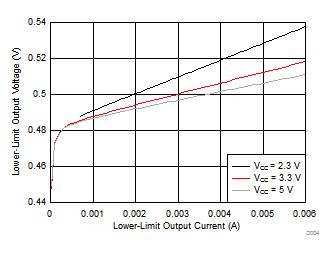
 Figure 1. Output Low Voltage (VOL) vs. Output Low Current (IOL) for SCL0 at Different VCC
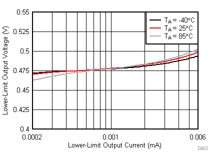
 Figure 2. Output Low Voltage (VOL) vs. Output Low Current (IOL) for SCL0 at Different Temperatures for VCC= 5 V