ZHCSNI7H September   2006  – March 2021 PCA9534

PRODUCTION DATA  

  1. 特性
  2. 说明
  3. Revision History
  4. Description (Continued)
  5. Device Comparison Table
  6. Pin Configuration and Functions
  7. Specifications
    1. 7.1 Absolute Maximum Ratings
    2. 7.2 ESD Ratings
    3. 7.3 Recommended Operating Conditions
    4. 7.4 Thermal Resistance Characteristics
    5. 7.5 Electrical Characteristics
    6. 7.6 I2C Interface Timing Requirements
    7. 7.7 Switching Characteristics
    8. 7.8 Typical Characteristics
  8. Parameter Measurement Information
  9. Detailed Description
    1. 9.1 Functional Block Diagram
    2. 9.2 Device Functional Modes
      1. 9.2.1 Power-On Reset
      2. 9.2.2 I/O Port
      3. 9.2.3 Interrupt Output ( INT)
        1. 9.2.3.1 Interrupt Errata
          1. 9.2.3.1.1 Description
          2. 9.2.3.1.2 System Impact
          3. 9.2.3.1.3 System Workaround
    3. 9.3 Programming
      1. 9.3.1 I2C Interface
      2. 9.3.2 Register Map
        1. 9.3.2.1 Device Address
        2. 9.3.2.2 Control Register And Command Byte
        3. 9.3.2.3 Register Descriptions
        4. 9.3.2.4 Bus Transactions
          1. 9.3.2.4.1 Writes
          2. 9.3.2.4.2 Reads
  10. 10Application Information Disclaimer
    1. 10.1 Application Information
      1. 10.1.1 Typical Application
        1. 10.1.1.1 Design Requirements
          1. 10.1.1.1.1 Minimizing ICC When The I/O Controls Leds
  11. 11Power Supply Recommendations
    1. 11.1 Power-On Reset Requirements
  12. 12Device and Documentation Support
    1. 12.1 Receiving Notification of Documentation Updates
    2. 12.2 Support Resources
    3. 12.3 Trademarks
    4. 12.4 Electrostatic Discharge Caution
    5. 12.5 Glossary
  13. 13Mechanical, Packaging, and Orderable Information

封装选项

机械数据 (封装 | 引脚)
散热焊盘机械数据 (封装 | 引脚)
订购信息

Typical Application

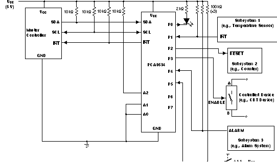
Figure 10-1 shows an application in which the PCA9534 can be used.
GUID-DE5294C8-C4CB-4F78-8FD4-6A14FB9C35D5-low.gif
Device address is configured as 0100100 for this example.
P0, P2, and P3 are configured as outputs.
P1, P4, and P5 are configured as inputs.
P6 and P7 are not used and must be configured as outputs.
Figure 10-1 Typical Application