ZHCSQB9H April 2006 – March 2022 PCA9536
PRODUCTION DATA
- 1 特性
- 2 应用
- 3 说明
- 4 Revision History
- 5 Pin Configuration and Functions
- 6 Specifications
- 7 Parameter Measurement Information
- 8 Detailed Description
- 9 Application Information Disclaimer
- 10Power Supply Recommendations
- 11Layout
- 12Device and Documentation Support
- 13Mechanical, Packaging, and Orderable Information
9.2.1.1 Minimizing ICC When I/Os Control LEDs
When the I/Os are used to control LEDs, they are normally connected to VCC through a resistor as shown in Figure 9-1. The LED acts as a diode so, when the LED is off, the I/O VIN is about 1.2 V less than VCC. The supply current, ICC, increases as VIN becomes lower than VCC and is specified as ΔICC in Electrical Characteristics.
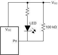
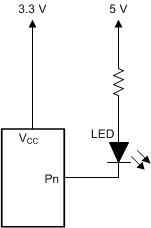
Designs needing to minimize current consumption, such as battery power applications, should consider maintaining the I/O pins greater than or equal to VCC when the LED is off. Figure 9-2 shows a high-value resistor in parallel with the LED. Figure 9-3 shows VCC less than the LED supply voltage by at least 1.2 V. Both of these methods maintain the I/O VIN at or above VCC and prevent additional supply-current consumption when the LED is off.
 Figure 9-2 High-Value Resistor in Parallel with the LED
 Figure 9-3 Device Supplied by a Lower Voltage