ZHCSHU7J August   2005  – March 2021 PCA9555

PRODUCTION DATA  

  1. 特性
  2. 应用
  3. 说明
  4. Revision History
  5. Pin Configuration and Functions
  6. Specifications
    1. 6.1 Absolute Maximum Ratings
    2. 6.2 ESD Ratings
    3. 6.3 Recommended Operating Conditions
    4. 6.4 Thermal Information
    5. 6.5 Electrical Characteristics
    6. 6.6 I2C Interface Timing Requirements
    7. 6.7 Switching Characteristics
    8. 6.8 Typical Characteristics
  7. Parameter Measurement Information
  8. Detailed Description
    1. 8.1 Overview
    2. 8.2 Functional Block Diagram
    3. 8.3 Device Features
      1. 8.3.1 Power-On Reset (POR)
      2. 8.3.2 I/O Port
    4. 8.4 Device Functional Modes
      1. 8.4.1 Interrupt ( INT) Output
        1. 8.4.1.1 Interrupt Errata
          1. 8.4.1.1.1 INT Description
          2. 8.4.1.1.2 System Impact
          3. 8.4.1.1.3 System Workaround
    5. 8.5 Programming
      1. 8.5.1 I2C Interface
      2. 8.5.2 Register Map
        1. 8.5.2.1 Device Address
        2. 8.5.2.2 Control Register And Command Byte
        3. 8.5.2.3 Register Descriptions
        4. 8.5.2.4 Bus Transactions
          1. 8.5.2.4.1 Writes
          2. 8.5.2.4.2 Reads
  9. Application Information Disclaimer
    1. 9.1 Application Information
      1. 9.1.1 Typical Application
        1. 9.1.1.1 Design Requirements
        2. 9.1.1.2 Design Requirements
          1. 9.1.1.2.1 Minimizing ICC When I/O Is Used To Control Led
        3. 9.1.1.3 Application Curves
  10. 10Power Supply Recommendations
    1. 10.1 Power-On Reset Requirements
  11. 11Layout
    1. 11.1 Layout Guidelines
    2. 11.2 Layout Example
  12. 12Device and Documentation Support
    1. 12.1 Receiving Notification of Documentation Updates
    2. 12.2 Support Resources
    3. 12.3 Trademarks
    4. 12.4 Electrostatic Discharge Caution
    5. 12.5 Glossary
  13. 13Mechanical, Packaging, and Orderable Information

封装选项

机械数据 (封装 | 引脚)
散热焊盘机械数据 (封装 | 引脚)
订购信息
Writes

Data is transmitted to the PCA9555 by sending the device address and setting the least-significant bit to a logic 0 (see Figure 8-6 for device address). The command byte is sent after the address and determines which register receives the data that follows the command byte.

The eight registers within the PCA9555 are configured to operate as four register pairs. The four pairs are input ports, output ports, polarity inversion ports, and configuration ports. After sending data to one register, the next data byte is sent to the other register in the pair (see Figure 8-8 and Figure 8-9). For example, if the first byte is sent to output port (register 3), the next byte is stored in Output Port 0 (register 2).

There is no limitation on the number of data bytes sent in one write transmission. In this way, each 8-bit register may be updated independently of the other registers.
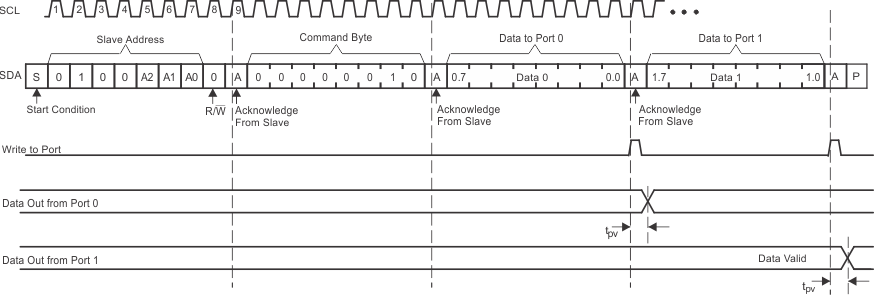
GUID-A7B62783-BCA1-4B58-B66A-3430F5BFC3CA-low.gifFigure 8-8 Write To Output Port Registers
GUID-AE139058-6371-4DDF-BEA8-44F8CCD217CC-low.gifFigure 8-9 Write To Configuration Registers