SBAS448B October 2008 – August 2015 PCM1690
PRODUCTION DATA.
- 1 Features
- 2 Applications
- 3 Description
- 4 Revision History
- 5 Pin Configuration and Functions
-
6 Specifications
- 6.1 Absolute Maximum Ratings
- 6.2 ESD Ratings
- 6.3 Recommended Operating Conditions
- 6.4 Thermal Information
- 6.5 Electrical Characteristics: Digital Input/Output
- 6.6 Electrical Characteristics: DAC
- 6.7 Electrical Characteristics: Power-Supply Requirements
- 6.8 System Clock Timing Requirements
- 6.9 Audio Interface Timing Requirements for Left-Justified, Right-Justified, and I2S Data Formats
- 6.10 Audio Interface Timing Requirements for DSP and TDM Data Formats
- 6.11 Three-Wire Serial Control Interface Timing Requirements
- 6.12 SCL and SDA Control Interface Timing Requirements
- 6.13 Typical Characteristics
-
7 Detailed Description
- 7.1 Overview
- 7.2 Functional Block Diagram
- 7.3
Feature Description
- 7.3.1 Analog Outputs
- 7.3.2 Voltage Reference VCOM
- 7.3.3 System Clock Input
- 7.3.4 Sampling Mode
- 7.3.5 Reset Operation
- 7.3.6 Zero Flag
- 7.3.7 AMUTE Control
- 7.3.8 Three-Wire (SPI) Serial Control
- 7.3.9 Control Data Word Format
- 7.3.10 Register Write Operation
- 7.3.11 Two-Wire (I2C) Serial Control
- 7.3.12 Packet Protocol
- 7.3.13 Write Operation
- 7.3.14 Read Operation
- 7.3.15 Timing Requirements: SCL and SDA
- 7.4 Device Functional Modes
- 7.5 Register Maps
- 8 Application and Implementation
- 9 Power Supply Recommendations
- 10Layout
- 11Device and Documentation Support
- 12Mechanical, Packaging, and Orderable Information
封装选项
请参考 PDF 数据表获取器件具体的封装图。
机械数据 (封装 | 引脚)
- DCA|48
散热焊盘机械数据 (封装 | 引脚)
- DCA|48
订购信息
8 Application and Implementation
NOTE
Information in the following applications sections is not part of the TI component specification, and TI does not warrant its accuracy or completeness. TI’s customers are responsible for determining suitability of components for their purposes. Customers should validate and test their design implementation to confirm system functionality.
8.1 Application Information
8.1.1 Lowpass Filter and Differential-to-Single-Ended Converter for DAC Outputs
ΔΣ DACs use noise-shaping techniques to improve in-band signal-to-noise ratio (SNR) performance at the expense of generating increased out-of-band noise above the Nyquist frequency, or fS/2. The out-of-band noise must be lowpass filtered in order to provide optimal converter performance. This filtering is accomplished by a combination of on-chip and external lowpass filters.
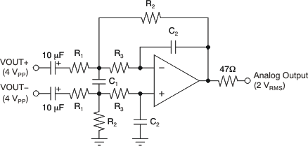
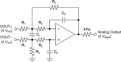
Figure 39 and Figure 40 show the recommended external differential-to-single-ended converter with lowpass active filter circuits for AC-coupled and DC-coupled applications. These circuits are second-order Butterworth filters using a multiple feedback (MFB) circuit arrangement that reduces sensitivity to passive component variations over frequency and temperature. For more information regarding MFB active filter designs, please refer to Applications Bulletin SBAA055, Dynamic Performance Testing of Digital Audio D/A Converters, available from the TI web site (www.ti.com) or the local Texas Instruments' sales office.
Because the overall system performance is defined by the quality of the DACs and the associated analog output circuitry, high-quality audio op amps are recommended for the active filters. Texas Instruments’ OPA2134, OPA2353, and NE5532A dual op amps are shown in Figure 39 and Figure 40, and are recommended for use with the PCM1690.


8.2 Typical Application
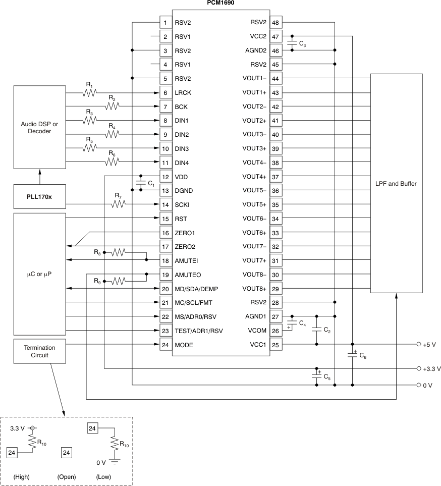
A basic connection diagram is shown in Figure 41, with the necessary power-supply bypassing and decoupling components. Texas Instruments’ PLL170X is used to generate the system clock input at SCKI, as well as to generate the clock for the audio signal processor. The use of series resistors (22 Ω to 100 Ω) are recommended for SCKI, LRCK, BCK, DIN1, DIN2, DIN3, and DIN4 for electromagnetic interference (EMI) reduction.

8.2.1 Design Requirements
- Control: Hardware, I2C, or SPI
- Audio Input: PCM Serial data, TDM, or DSP
- Audio Output: (1.6 × VCC1) Vpp analog audio biased to (0.5 × VCC1) V
- Master Clock: PLL170X IC
8.2.2 Detailed Design Procedure
8.2.2.1 Hardware Control Method
There are 3 ways to control the PCM1690, hardware control, SPI, or I2C. Hardware control will provide a limited access to control features available in the PCM1690 but can be implemented with pull up and pull downs, or with GPIO of a microcontroller. Control via SPI or I2C will provide access to all control registers and features but will require a digital device that can implement SPI or I2C.
8.2.2.2 Audio Input
For Audio Input there are 3 options, PCM serial data, TDM, or DSP. All three will support the same quality of audio data, but having these 3 options to match the audio sources available outputs allows for greater flexibility. This selection is made by configuring the MODE pin which is detailed in Table 6 and shown in Pin Functions.
8.2.2.3 Audio Output
The output of the PCM1690 will produce a differential (1.6 × VCC1) Vpp signal at full scale into a 5-kΩ load, that must be filtered before being sent to an amplifier. Outputs Vout1 through Vout 8 will be biased at (0.5 × VCC1) V.
8.2.2.4 Master Clock
The master clock can come from wither a dedicated IC such as the PLL170X series, a crystal or the audio source IC. What is important is that the audio source and the PCM1690 are driven from the same source so that the audio clocks will be synchronous.
8.2.3 Application Curve
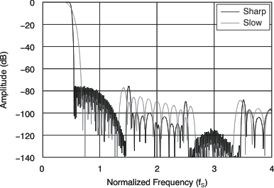
 Figure 42. Frequency Response
(Single Rate)