SBAS448B October 2008 – August 2015 PCM1690
PRODUCTION DATA.
- 1 Features
- 2 Applications
- 3 Description
- 4 Revision History
- 5 Pin Configuration and Functions
-
6 Specifications
- 6.1 Absolute Maximum Ratings
- 6.2 ESD Ratings
- 6.3 Recommended Operating Conditions
- 6.4 Thermal Information
- 6.5 Electrical Characteristics: Digital Input/Output
- 6.6 Electrical Characteristics: DAC
- 6.7 Electrical Characteristics: Power-Supply Requirements
- 6.8 System Clock Timing Requirements
- 6.9 Audio Interface Timing Requirements for Left-Justified, Right-Justified, and I2S Data Formats
- 6.10 Audio Interface Timing Requirements for DSP and TDM Data Formats
- 6.11 Three-Wire Serial Control Interface Timing Requirements
- 6.12 SCL and SDA Control Interface Timing Requirements
- 6.13 Typical Characteristics
-
7 Detailed Description
- 7.1 Overview
- 7.2 Functional Block Diagram
- 7.3
Feature Description
- 7.3.1 Analog Outputs
- 7.3.2 Voltage Reference VCOM
- 7.3.3 System Clock Input
- 7.3.4 Sampling Mode
- 7.3.5 Reset Operation
- 7.3.6 Zero Flag
- 7.3.7 AMUTE Control
- 7.3.8 Three-Wire (SPI) Serial Control
- 7.3.9 Control Data Word Format
- 7.3.10 Register Write Operation
- 7.3.11 Two-Wire (I2C) Serial Control
- 7.3.12 Packet Protocol
- 7.3.13 Write Operation
- 7.3.14 Read Operation
- 7.3.15 Timing Requirements: SCL and SDA
- 7.4 Device Functional Modes
- 7.5 Register Maps
- 8 Application and Implementation
- 9 Power Supply Recommendations
- 10Layout
- 11Device and Documentation Support
- 12Mechanical, Packaging, and Orderable Information
封装选项
请参考 PDF 数据表获取器件具体的封装图。
机械数据 (封装 | 引脚)
- DCA|48
散热焊盘机械数据 (封装 | 引脚)
- DCA|48
订购信息
10 Layout
10.1 Layout Guidelines
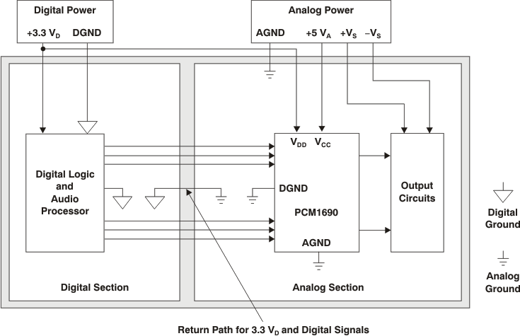
A typical printed-circuit-board (PCB) layout for the PCM1690 is shown in Figure 43. A ground plane is recommended, with the analog and digital sections being isolated from one another using a split or cut in the circuit board. The PCM1690 must be oriented with the digital I/O pins facing the ground plane split/cut to allow for short, direct connections to the digital audio interface and control signals originating from the digital section of the board.
Separate power supplies are recommended for the digital and analog sections of the board. This configuration prevents the switching noise present on the digital supply from contaminating the analog power supply and degrading the dynamic performance of the PCM1690.
10.2 Layout Example
 Figure 43. Recommended PCB Layout