ZHCSK28E April 2003 – July 2019 PCM1753 , PCM1754 , PCM1755
PRODUCTION DATA.
- 1 特性
- 2 应用
- 3 说明
- 4 修订历史记录
- 5 Device Comparison Table
- 6 Pin Configuration and Functions
- 7 Specifications
-
8 Detailed Description
- 8.1 Overview
- 8.2 Functional Block Diagram
- 8.3 Feature Description
- 8.4 Device Functional Modes
- 8.5 Programming
- 8.6
Register Maps
- 8.6.1
Mode Control Registers (PCM1753/55)
- 8.6.1.1 User-Programmable Mode Controls
- 8.6.1.2
Register Definitions
- 8.6.1.2.1 ATx[7:0]: Digital Attenuation Level Setting
- 8.6.1.2.2 MUTx: Soft Mute Control
- 8.6.1.2.3 OVER: Oversampling Rate Control
- 8.6.1.2.4 SRST: Reset
- 8.6.1.2.5 DACx: DAC Operation Control
- 8.6.1.2.6 DM12: Digital De-Emphasis Function Control
- 8.6.1.2.7 DMF[1:0]: Sampling Frequency Selection for the De-Emphasis Function
- 8.6.1.2.8 FMT[2:0]: Audio Interface Data Format
- 8.6.1.2.9 FLT: Digital Filter Rolloff Control
- 8.6.1.2.10 DREV: Output Phase Select
- 8.6.1.2.11 ZREV: Zero Flag Polarity Select
- 8.6.1.2.12 AZRO: Zero Flag Function Select
- 8.6.1
Mode Control Registers (PCM1753/55)
- 9 Application and Implementation
- 10Power Supply Recommendations
- 11Layout
- 12器件和文档支持
- 13机械、封装和可订购信息
9.2.1.3 D/A Output Filter Circuits
Delta-sigma D/A converters use noise-shaping techniques to improve in-band signal-to-noise ratio (SNR) performance at the expense of generating increased out-of-band noise above the Nyquist frequency, or fS/2. The out-of-band noise must be low-pass filtered in order to provide the optimal converter performance. This is accomplished by a combination of on-chip and external low-pass filtering.
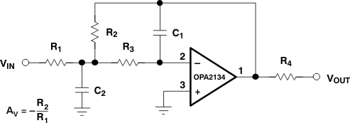
Figure 25(a) and Figure 31 show the recommended external low-pass active filter circuits for single- and dual-supply applications. These circuits are 2nd-order Butterworth filters using the multiple feedback (MFB) circuit arrangement, which reduces sensitivity to passive component variations over frequency and temperature. For more information regarding MFB active filter design, see Burr-Brown applications bulletin (SBAA055), available from the TI Web site at http://www.ti.com.
Because the overall system performance is defined by the quality of the D/A converters and their associated analog output circuitry, high-quality audio operational amplifiers are recommended for the active filters. TI's OPA2353 and OPA2134 dual operational amplifiers are shown in Figure 25(a) and Figure 31, and are recommended for use with the PCM1754 device.
 Figure 31. Dual-Supply Filter Circuit